Process and system for the verification of correct functioning of an on-chip memory

a technology of correct functioning and process, applied in the direction of information storage, electronic circuit testing, instruments, etc., can solve the problems of increasing laborious and laborious, bist system itself generating error flags, and existing bist may no longer be self-testable, etc., to improve the cost-efficiency of manufacturing and reduce the cost of adaptation of bist circuitry of the complex devi

Active Publication Date: 2012-04-17
STMICROELECTRONICS SRL
View PDF6 Cites 0 Cited by
  • Summary
  • Abstract
  • Description
  • Claims
  • Application Information

AI Technical Summary

Benefits of technology

[0017]The process of definition and implementation and a now found architecture for an on-chip BIST system for a nonvolatile read only memory, programmable one or more times, may effectively overcome these drawbacks and constraints.
[0021]According to a preferred embodiment, particularly useful for nonvolatile memories that are electrically programmable one or more times, even the dedicated nonvolatile storage block in which the specifically calculated control signature is recorded is electrically programmable / reprogrammable, such that the control signature itself can be updated every time the manufacturer of the devices and / or the user write a different code in the ROM. It is thus possible to carry out the indispensable control of correctness of a newly recorded ROM code still using the same BIST logic circuitry that was realized in the device even if the new ROM code is different from the code originally initially contemplated by the designer / manufacturer of the device.
[0024]The value of the control signature, recalculated for a modified ROM code, can be stored in the dedicated nonvolatile storage block without requiring any change of the circuit components of the logic self-test machine. It may be sufficient to connect the processing “core” circuitry that calculates the signature to the storage block of the control signature through controlled switches, to be turned on for modifying the non volatily stored control signature when it is recalculated for a new ROM code stored in the nonvolatile memory. In the case of a ROM type nonvolatile supports, that are one-time programmable by defining interconnections and / or electric paths in a metal layer of the device being fabricated, even the value of the control signature may be recorded in an advanced phase of the fabrication process, with an evidently enhanced cost-efficiency of manufacturing.
[0025]When the value of the control signature is stored in the BIST system at the same time the ROM code is programmed in the on-chip memory, costs of adaptation of the design of the BIST circuitry of the complex device to new uses and / or applications are eliminated.

Problems solved by technology

The ever increasing complexity of integrated circuits, the quest for more specialized functions, and the characteristics and performances of which must satisfy stringent specifications imposed by the user / customer make the verification of devices for testing whether they are compliant or not with specifications increasingly difficult and laborious.
If the control signature stored in the BIST system does not match the signature resulting from the execution of the self-test, the BIST system itself generates an error flag (test failed).
Indeed, according to these cost efficient embodiments of BIST modules, the same logic machine may be unusable with a different ROM code to be stored in the memory at the time of late programming the ROM according to possibly modified customer's request.
If the ROM code may be changed for complying with special customer requirements, the existing BIST may no longer be self-testable because it is helpful to modify the logic circuit of the BIST, with an attendant increase of costs for accordingly modifying the fabrication process during front-end phases for making the functions of the BIST compliant with the different ROM code that is requested.
When an on-chip ROM memory may be programmed with a different code from the original design code, the BIST module implemented on the basis of a certain ROM code, may be no longer able to verify the functionality of the memory in which a different ROM code has been stored.
This may be significant in the case of complex SoC devices, because during the design of the device it may happen that the ROM code is modified and in these cases it may be likely that the already realized respective BIST module may not be compliant with it.
In all these cases the new ROM code may be helpfully verified by connecting the device to a test machine, because the self-test BIST structure integrated on the chip may no longer be useful, thus resulting in long verification times and related costs.

Method used


Image

  • Process and system for the verification of correct functioning of an on-chip memory
  • Process and system for the verification of correct functioning of an on-chip memory
  • Process and system for the verification of correct functioning of an on-chip memory

Examples


Embodiment Construction

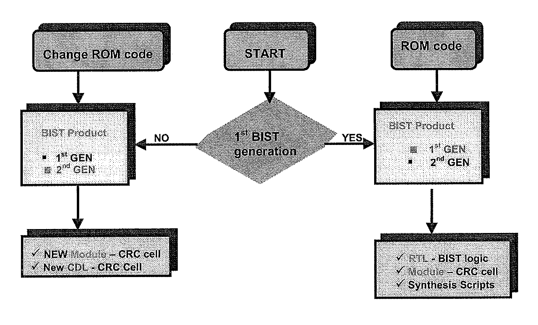
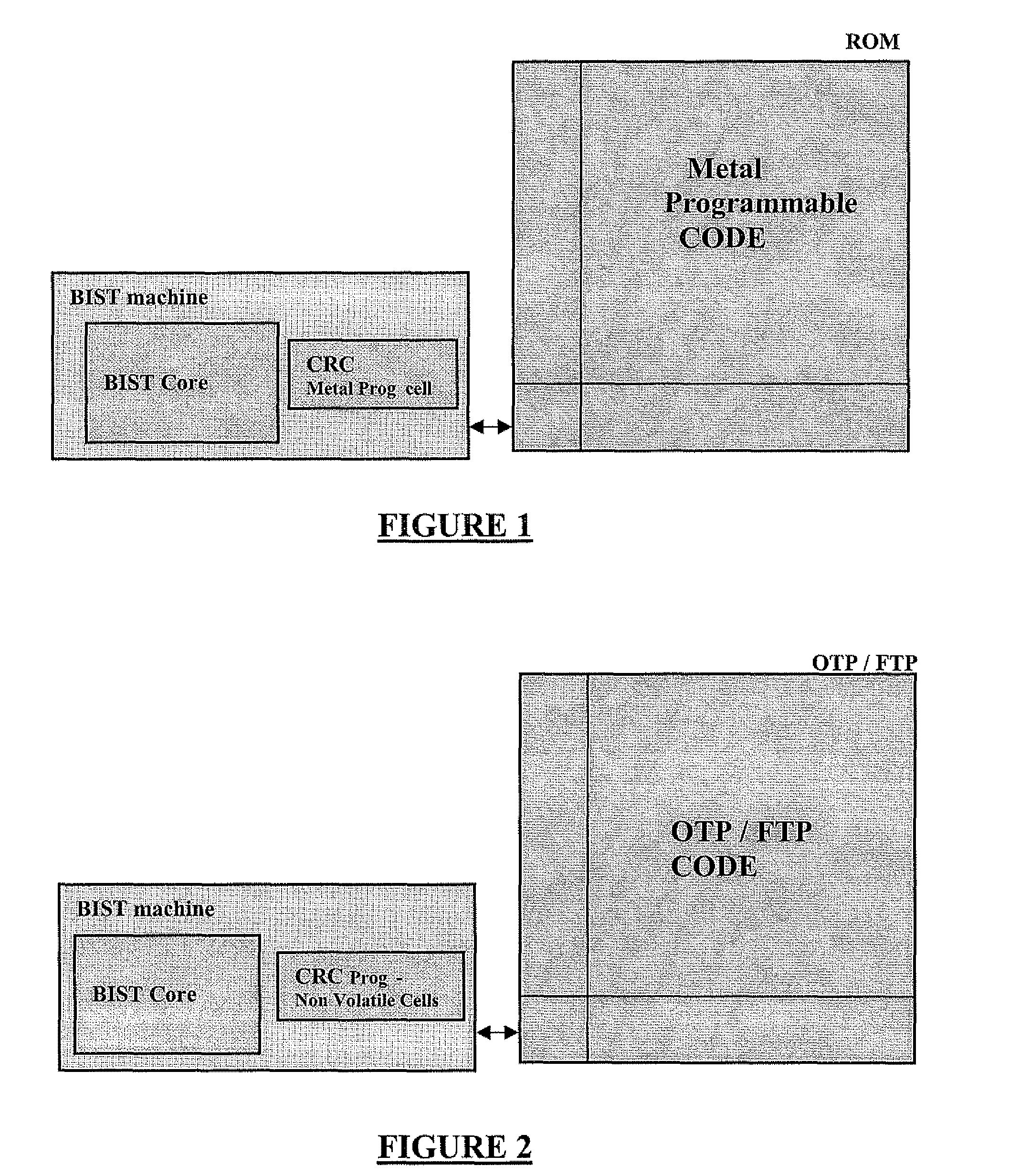
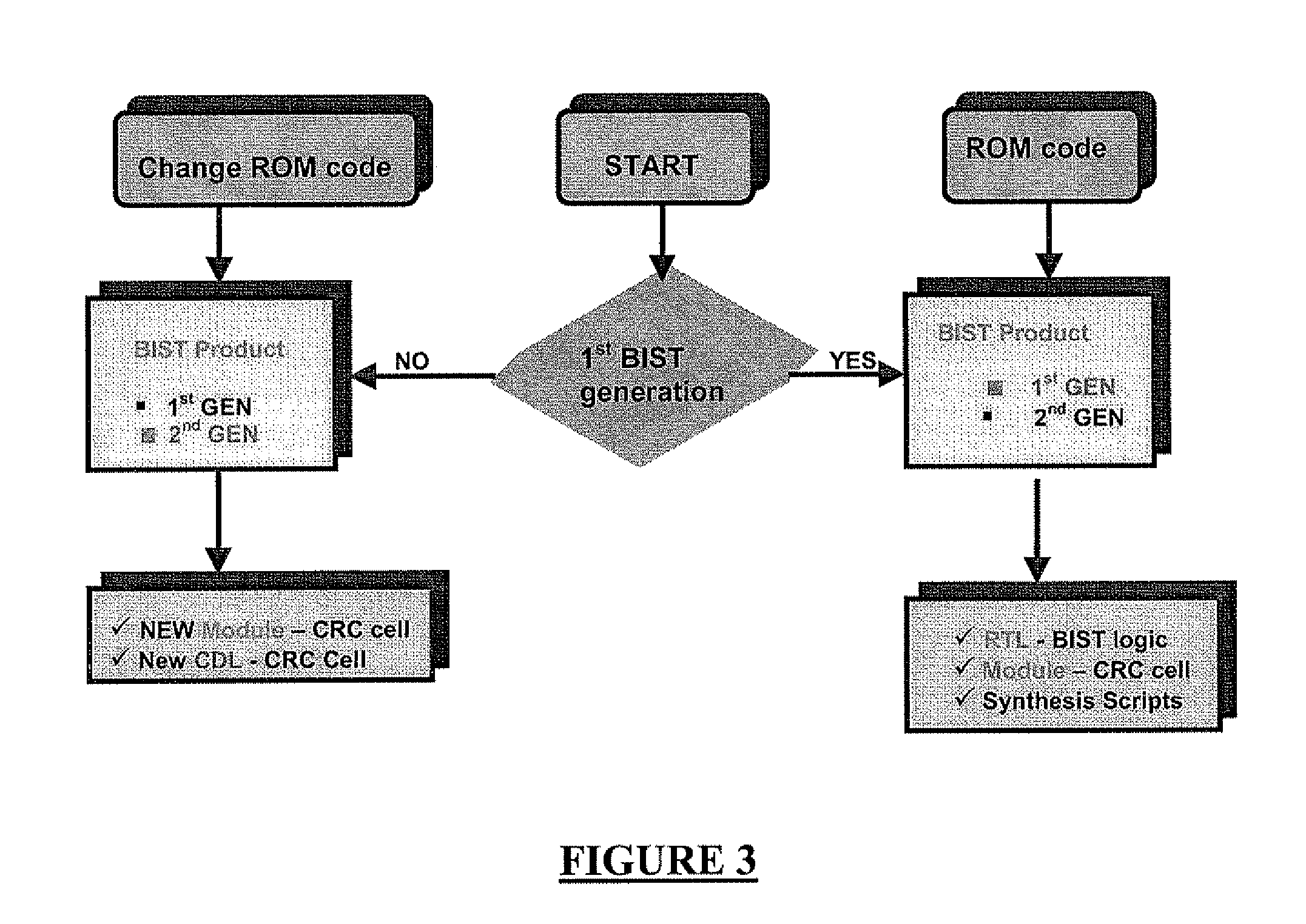
[0028]The diagrams of FIGS. 1 and 2 illustrate exemplary architectures of BIST systems according to this approach for self-testing the functionality of a nonvolatile memory (ROM, OTP or FTP) storing a certain ROM code, including a prior defined and implemented logic processing machine (BIST Core) capable of calculating a signature for the ROM code as stored in the memory, in order to verify the correct functioning of the nonvolatile memory, and a dedicated nonvolatile storage block (CRC), rewritable or not, coupled to the BIST Core circuitry, in which is recorded the value of a control signature that has been specifically calculated for the ROM code to be stored in the memory (ROM, OTP or FTP) of the devices being fabricated.

[0029]The logic circuitry (BIST Core) of the BIST system is realized in the device during a front-end phase of the fabrication process, whilst the specific control signature for the ROM code to be stored in the memory (ROM, OTP or FTP) is recorded at a later pha...


PUM


Abstract

A method is for making an integrated circuit with built-in self-test. The method includes forming at least one nonvolatile read only memory (ROM) to store ROM code and forming a logic self-test circuit to verify a correct functioning of the at least one nonvolatile ROM. Moreover, the method includes defining, in the logic self-test circuit, a logic self-test core to process the ROM code and to generate a flag based upon a control signature and defining, in the logic self-test circuit, a nonvolatile storage block, coupled to the logic self-test core, to store the control signature. Furthermore, the method includes writing the ROM code to the at least one nonvolatile ROM and writing the control signature to the nonvolatile storage block, during a same fabrication step.

Description

FIELD OF THE INVENTION[0001]This invention relates in general to the fabrication of very large integration scale systems, for example SoCs (System-on-Chip) or ASICs (Application Specific Integrated Circuit), embodied in a nonvolatile memory device, and, more particularly, to devices including a logic machine defined BIST or M-BIST (memory built-in self testing) for the verification of correct functioning of a nonvolatile memory device that uses a control signature, or more briefly a signature, stored in the same logic machine integrated in the device.BACKGROUND OF THE INVENTION[0002]The ever increasing complexity of integrated circuits, the quest for more specialized functions, and the characteristics and performances of which must satisfy stringent specifications imposed by the user / customer make the verification of devices for testing whether they are compliant or not with specifications increasingly difficult and laborious. The need of developing testing methods and technologies ...

Claims


Application Information

Patent Timeline
Patent Type & Authority Patents(United States)
IPC IPC(8): G06F11/00
CPCG01R31/3187G06F11/1004G11C29/40G11C17/14G11C2029/0401G11C2029/4402
Inventor SELVA, CAROLINATORELLI, COSIMORIMONDI, DANILOZAPPA, RITA
Owner STMICROELECTRONICS SRL
Why Eureka
Try Eureka