Method of manufacturing MEMS sensor and MEMS sensor

a manufacturing method and sensor technology, applied in the direction of instruments, semiconductor electrostatic transducers, acceleration measurement using interia forces, etc., can solve the disadvantage of protective film etching, and achieve the effect of preventing adhesion

Inactive Publication Date: 2012-05-08
ROHM CO LTD
View PDF63 Cites 17 Cited by
  • Summary
  • Abstract
  • Description
  • Claims
  • Application Information

AI Technical Summary

Benefits of technology

[0009]An object of the present invention is to provide a method of manufacturing an MEMS sensor and an MEMS sensor, capable of preventing undesired etching of a protective film made of a nonmetallic material.
[0013]The nonmetallic material is employed for the protective film, and the metallic material is employed for the second sacrificial layer. Therefore, the etching selection ratio of the protective film to the second sacrificial layer can be easily increased. When the second sacrificial layer is made of a metallic material containing Al (aluminum) and the protective film is made of an organic material, for example, the etching selection ratio of the protective film to the second sacrificial layer can be increased by employing chlorine-based gas as the etchant for etching the second sacrificial layer. Consequently, etching of the protective film can be prevented even if the protective film is exposed to the chlorine-based gas over a long period when the second sacrificial layer is etched.
[0018]The upper electrode is made of TiN, TiW, Cr or W, whereby a metallic material containing Al can be employed as the material for the second sacrificial layer formed for manufacturing the MEMS sensor. TiN, TiW, Cr or W is a relatively hard metallic material. When the metallic material is employed for the upper electrode, therefore, high strength can be ensured for the upper electrode.

Problems solved by technology

However, a relatively long time (20 to 30 minutes, for example) is required for removing the lower and upper sacrificial layers while the protective film is also exposed to the hydrofluoric acid over the long time, and hence the protective film is disadvantageously etched.

Method used


Image

  • Method of manufacturing MEMS sensor and MEMS sensor
  • Method of manufacturing MEMS sensor and MEMS sensor
  • Method of manufacturing MEMS sensor and MEMS sensor

Examples


Embodiment Construction

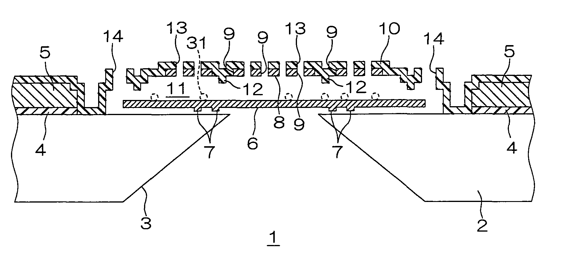
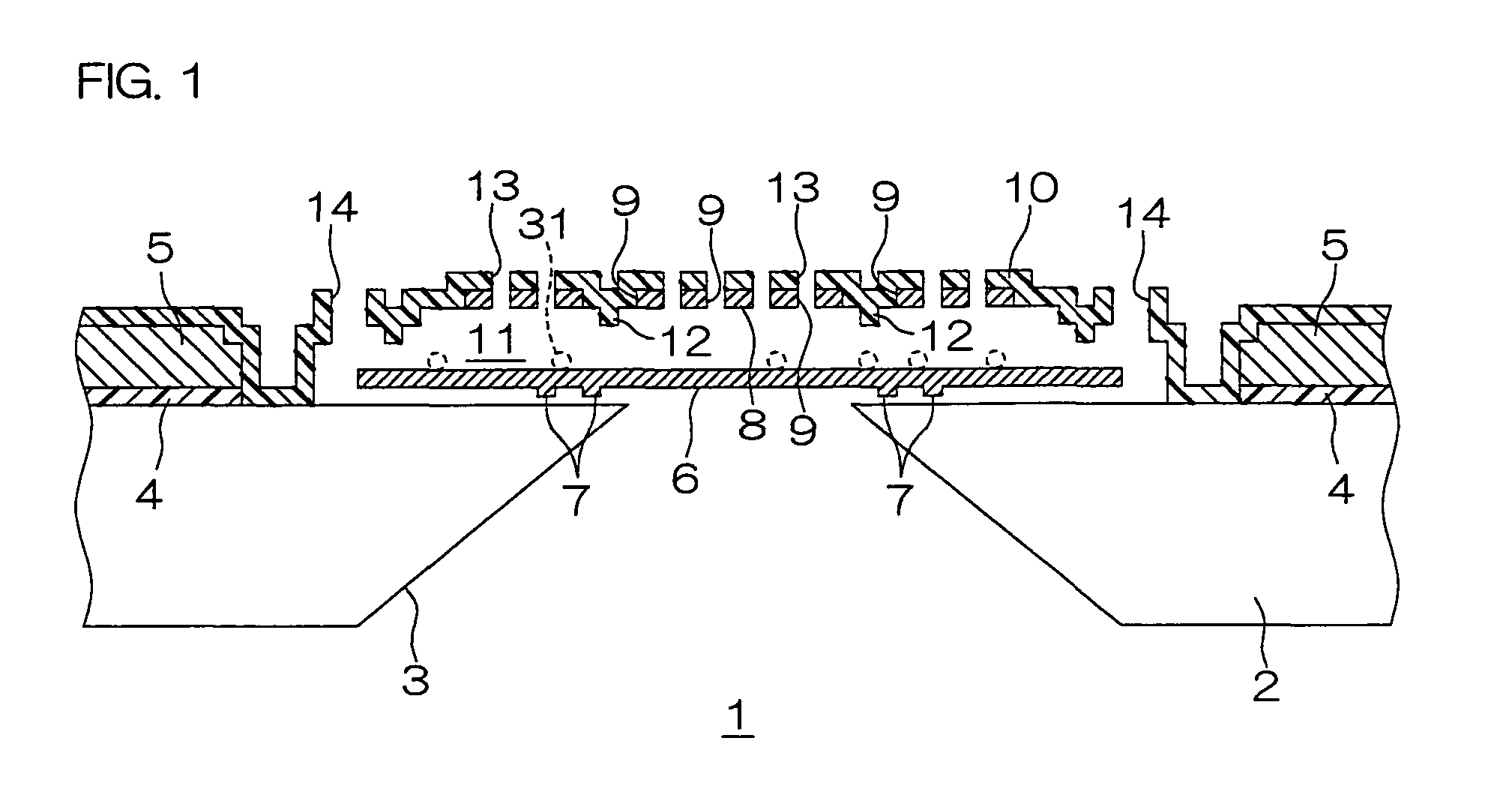
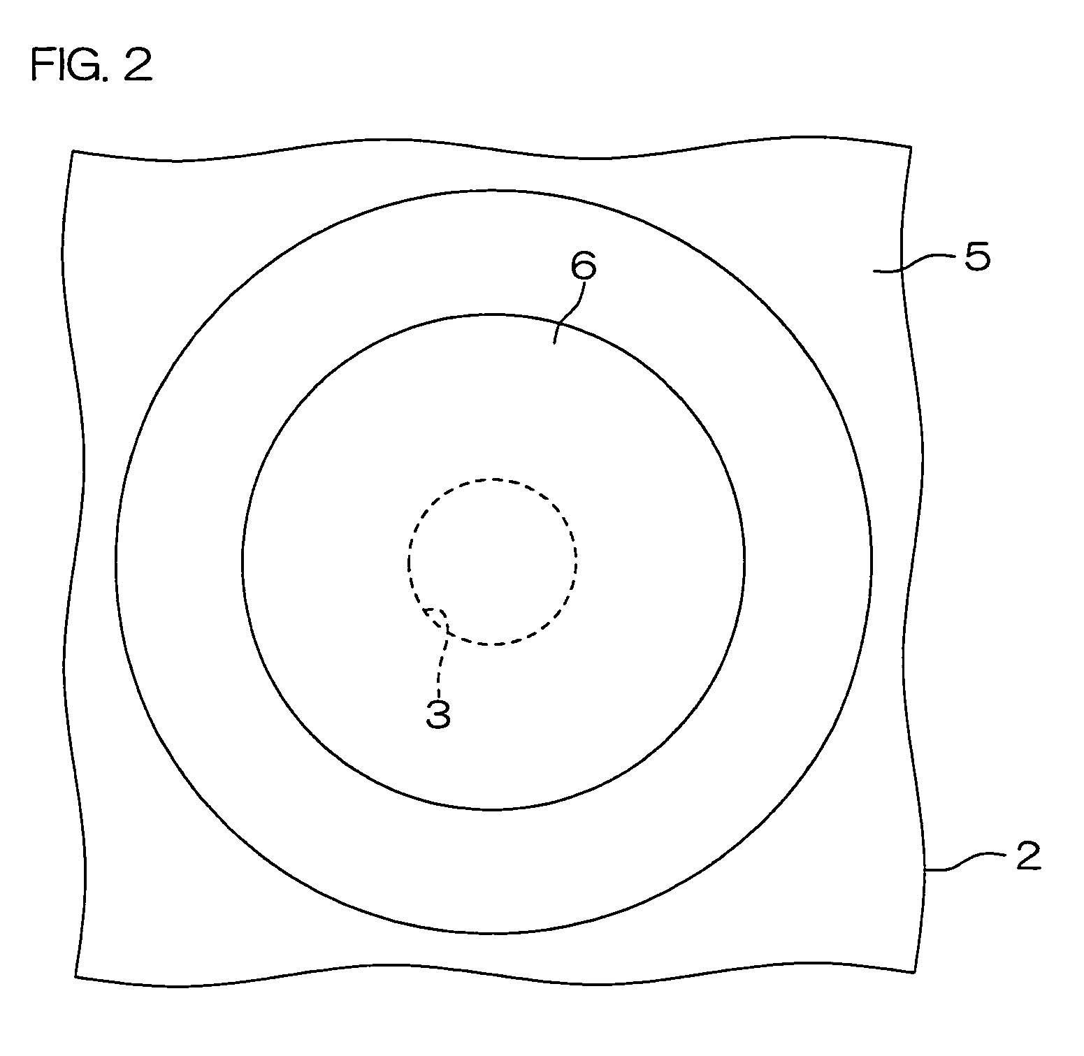
[0027]FIG. 1 is a schematic sectional view of a silicon microphone according to an embodiment of the present invention. FIG. 2 is a schematic plan view of the silicon microphone shown in FIG. 1.

[0028]A silicon microphone 1 is a sensor (an MEMS sensor) manufactured by the MEMS technique. The silicon microphone 1 includes a substrate 2 made of silicon. A through-hole 3 having a trapezoidal sectional shape narrowed toward the surface (the upper surface) (spreading toward the rear surface) is formed on a central portion of the substrate 2.

[0029]An insulating film 4 and a metal film 5 are stacked on the substrate 2 in this order from the side closer to the substrate 2. The insulating film 4 is made of SiO2, for example. The metal film 5 is made of Al, for example. The insulating film 4 and the metal film 5 are partially removed from a region including the through-hole 3 in plan view, and the surface of the substrate 2 is exposed in the region.

[0030]A diaphragm 6 in the form of a thin cir...


PUM

PropertyMeasurementUnit
adhesionaaaaaaaaaa
diameteraaaaaaaaaa
thicknessaaaaaaaaaa

Abstract

A method of manufacturing an MEMS sensor according to the present invention includes the steps of: forming a first sacrificial layer on one surface of a substrate; forming a lower electrode on the first sacrificial layer; forming a second sacrificial layer made of a metallic material on the first sacrificial layer to cover the lower electrode; forming an upper electrode made of a metallic material on the second sacrificial layer; forming a protective film made of a nonmetallic material on the substrate to collectively cover the first sacrificial layer, the second sacrificial layer and the upper electrode; and removing at least the second sacrificial layer by forming a through-hole in the protective film and supplying an etchant to the inner side of the protective film through the through-hole.

Description

BACKGROUND OF THE INVENTION[0001]1. Field of the Invention[0002]The present invention relates to a sensor (an MEMS sensor) manufactured by an MEMS (Micro Electro Mechanical Systems) technique and a method of manufacturing the same.[0003]2. Description of Related Art[0004]An MEMS sensor, having been recently loaded on a portable telephone or the like, is increasingly watched with interest. For example, a silicon microphone (an Si microphone) is a typical example of the MEMS sensor.[0005]The silicon microphone includes a silicon substrate. A through-hole is formed on a central portion of the silicon substrate, to penetrate the silicon substrate in the thickness direction. On the silicon substrate, a diaphragm made of polysilicon is arranged on a position opposed to the through-hole. The diaphragm is provided in a state floating up from the silicon substrate (at a small interval from the surface of the silicon substrate), to be vibratile in a direction opposed to the surface of the sil...

Claims


Application Information

Patent Timeline
Patent Type & Authority Patents(United States)
IPC IPC(8): H01L29/84
CPCG01L9/0042G01L9/0073B81B3/001B81C1/00476B81C1/00595B81B2201/0235B81B2201/0257B81B2201/0264H04R19/005B81C2201/0107
Inventor NAKATANI, GORO
Owner ROHM CO LTD
Why Eureka
Try Eureka