

Semiconductor device
a technology of a semiconductor and a feedback capacitance, applied in the direction of semiconductor devices, basic electric elements, electrical equipment, etc., to achieve the effect of reducing the amount of output capacitance and feedback capacitan
- Summary
- Abstract
- Description
- Claims
- Application Information
AI Technical Summary
Benefits of technology
Problems solved by technology
Method used
Image

Examples
first embodiment
[0055](First Embodiment)
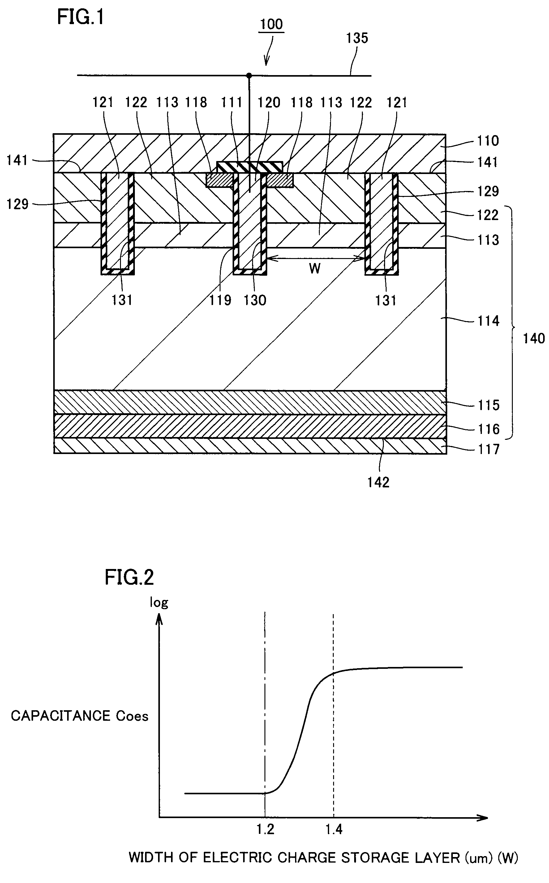
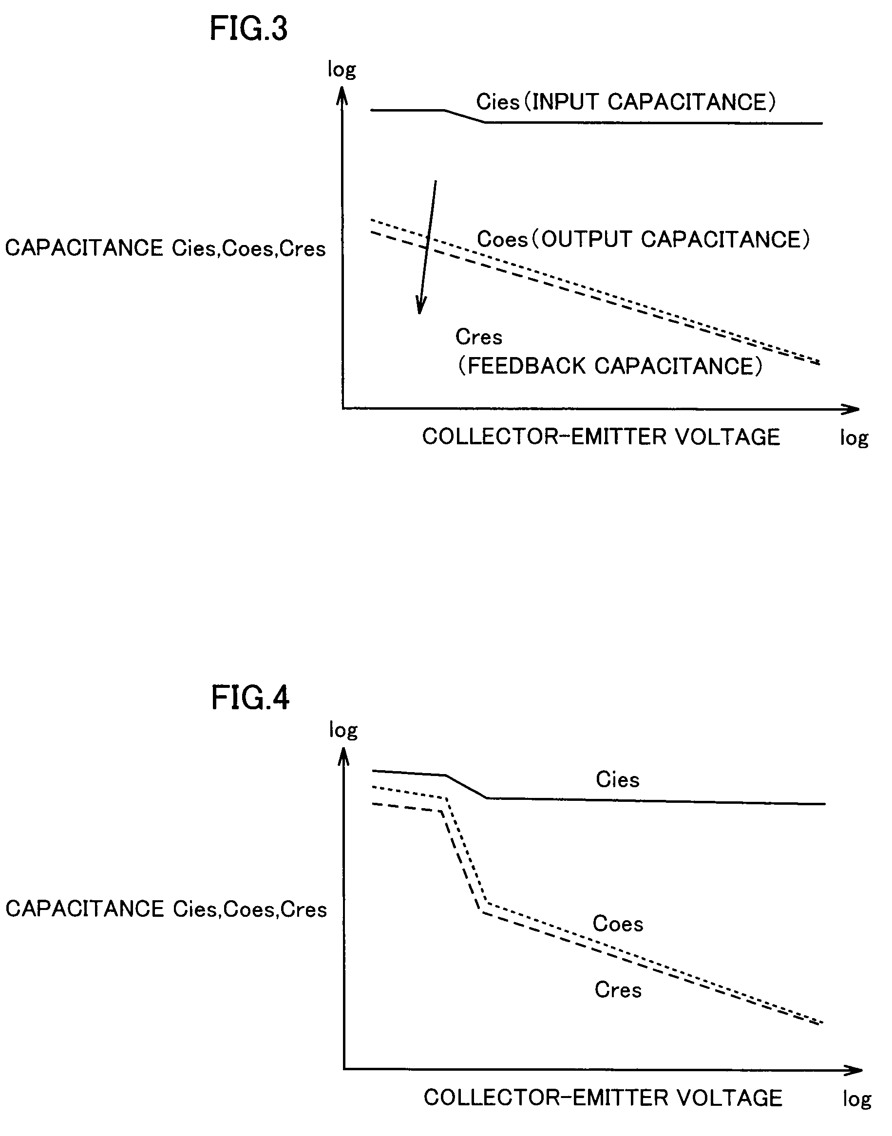
[0056]With the use of FIG. 1 to FIG. 4, a semiconductor device according to an embodiment of the present invention will be described. FIG. 1 is a cross-sectional view of a trench-type insulated gate semiconductor device 100 according to a first embodiment of the present invention. As shown in FIG. 1, trench-type insulated gate semiconductor device 100 includes a semiconductor substrate 140 that has a main surface 141 and a main surface 142 located on a side opposite to main surface 141, an n− semiconductor base (first impurity region) 114 of an n-type (first conductivity type) formed between main surface 141 and main surface 142, and a P collector layer (second impurity region) 116 of a p-type (second conductivity type) formed at main surface 142.
[0057]A collector electrode 117 is formed on main surface 142 and connected to P collector layer 116. Further, at a portion inside semiconductor substrate 140 adjacent to P collector layer 116 on a side opposite to c...
second embodiment
[0089](Second Embodiment)
[0090]With the use of FIG. 5 to FIG. 11, trench-type insulated gate semiconductor device 100 according to an embodiment of the present invention and a method of manufacturing the same will be described.
[0091]Note that in FIG. 5 to FIG. 11, the configurations same as or corresponding to the configurations shown in FIG. 1 to FIG. 4 described above are provided with the same reference characters, and the description thereof will not be repeated.
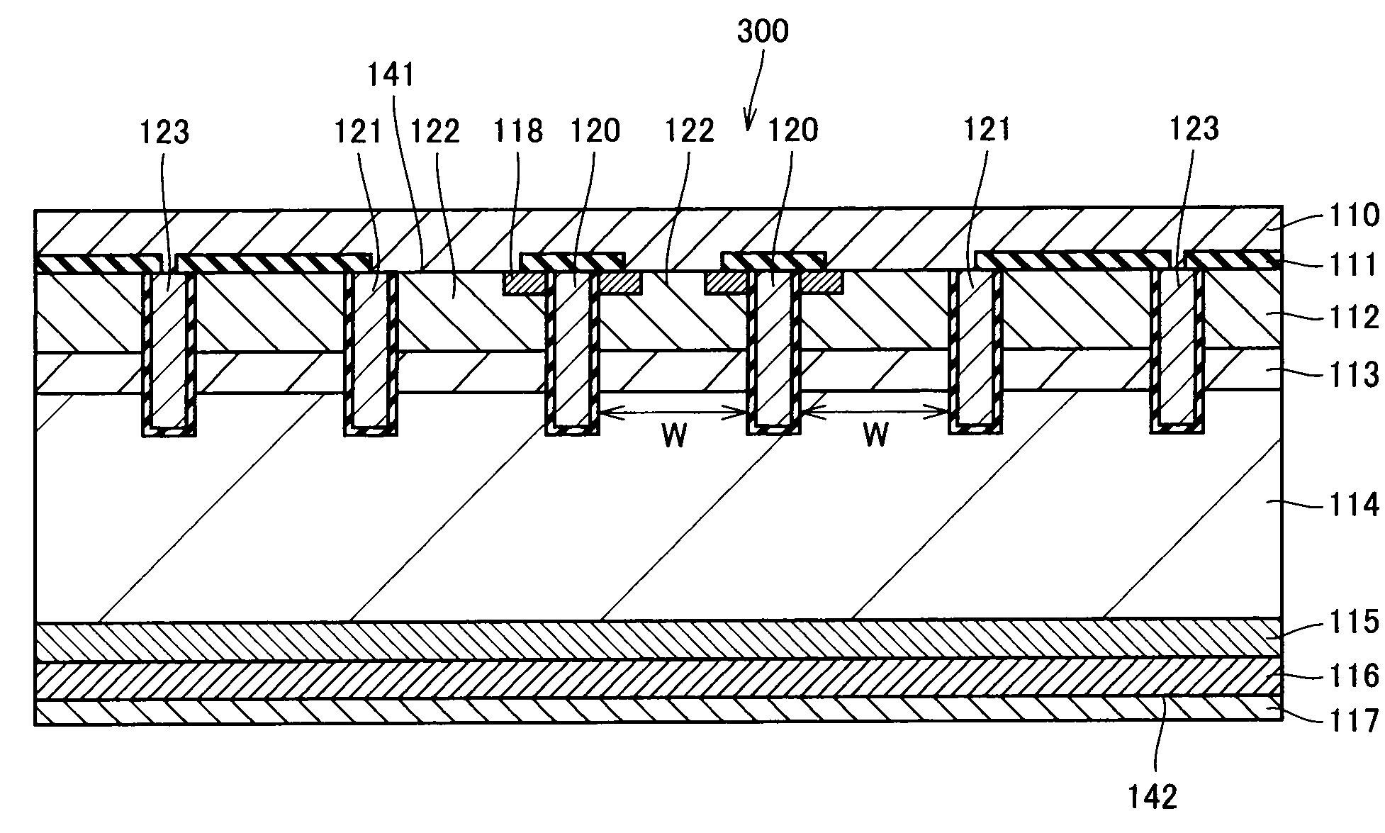
[0092]FIG. 5 is a cross-sectional view of trench-type insulated gate semiconductor device 100 according to a second embodiment of the present invention. As shown in FIG. 5, a cell 300 of trench-type insulated gate semiconductor device 100 includes gate electrode 120 connected to gate wiring 135, dummy gates 121 provided apart from gate electrode 120 on opposite sides of gate electrode 120, P base region 122 provided between gate electrode 120 and dummy gate 121 and connected to emitter electrode 110, and emitter layer 11...
third embodiment
[0110](Third Embodiment)
[0111]With the use of FIG. 12, trench-type insulated gate semiconductor device 100 according to a third embodiment of the present invention will be described. Note that in FIG. 12, the configurations same as or corresponding to the configurations shown in FIG. 1 to FIG. 11 described above are provided with the same reference characters, and the description thereof may not be repeated.
[0112]As shown in FIG. 12, trench-type insulated gate semiconductor device 100 includes a plurality of cells 300 disposed apart from one another.
[0113]Cell 300 includes gate electrode 120 connected to gate wiring 135, dummy gates 121 disposed apart from gate electrode 120 on the opposite sides thereof, P base region 122 located between gate electrode 120 and dummy gate 121, and emitter layer 118 located on P base region 122 and formed on each of the opposite sides of gate electrode 120. Floating region (sixth impurity region) 112 is formed on a side opposite to P base region 122 ...
PUM
 Abstract
Description
Claims
Application Information