Communication system and timing control method

a communication system and timing control technology, applied in the field of communication systems, can solve the problems of inability to retime photons, inability to optimize their own modulation timing, and loss of most data transmitted from senders, so as to facilitate the optimization of its own modulation timing, stable phase modulation and photon detection, and fast stable distribution of cryptographic keys

Active Publication Date: 2012-05-22
NEC CORP
View PDF7 Cites 14 Cited by
  • Summary
  • Abstract
  • Description
  • Claims
  • Application Information

AI Technical Summary

Benefits of technology

[0022]Therefore, an object of the present invention is to solve the above-described conventional problems. In particular, an object of the present invention is to provide a communication system and a timing control method that optimize timing in a sender and thereby enable information to be transmitted stably at the right timing.
[0023]Moreover, another object of the present invention is to provide an optical communication system that compensates for the group velocity dispersions in the case where an optical signal to be subjected to phase modulation and a clock signal are transmitted by wavelength division multiplexing transmission, and thereby drives the phase modulator at the right timing, thus enabling fast stable distribution of a cryptographic key.
[0027]As described above, the modulation timing of the first communication device is controlled by the second communication device and the second communication device can easily optimize its own modulation timing by monitoring the detection results obtained from the controlled modulation timing of the first communication device.
[0034]As described above, according to the present invention, the modulation timing of the first communication device is controlled by the second communication device and the second communication device can easily optimize its own modulation timing by monitoring the detection results obtained from the controlled modulation timing of the first communication device.
[0035]According to an embodiment of the present invention, the phase modulation timing of a transmitted is shifted by one step under control of a receiver and, every time one step is shifted, the receiver stores the detection result obtained from the received phase-modulated signal. Based on the stored detection result data, the receiver can determine the optimal timing of phase modulation of the sender. Accordingly, the receiver can confirm that the phase modulation timing of the sender is right, allowing the driving timing of a photon detector at the receiver to precisely coincide with the photon incident timing. This means that group velocity dispersions (GVD) due to wavelength-division multiplexing of phase-modulated optical signal and a clock signal can be compensated for. In other words, the phase modulator can be driven at stable modulation timing, resulting in desired phase modulation of an optical carrier signal.
[0036]In addition, an optical communication system according to the present invention can achieve stable phase modulation and photon detection. Accordingly, in the case of the present invention applied to a quantum key distribution system, it can compensate for timing difference between an optical signal and a clock signal due to wavelength distribution in the case where the optical signal to be subjected to phase modulation and the clock signal are transmitted by wavelength division multiplexing transmission, and thereby drives the phase modulator at the right timing, thus enabling fast stable distribution of a cryptographic key.

Problems solved by technology

Therefore, most of data transmitted from a sender is lost due to losses attributable to a transmission line, and little data arrives at a receiver.
In addition to this, photons cannot be retimed because the values of arriving data are probabilistically determined.
However, when the quantum signal and clock signal are transmitted by wavelength division multiplexing transmission, a propagation delay difference arises because the different-wavelength channels have different group velocity dispersions (GVD).
Such a propagation delay difference between channels is a grave problem to solve, for a system that requires synchronization between different-channel signals.
Additionally, in a system that transmits information by utilizing phase modulation, such as a quantum key distribution system as described above, it cannot be determined whether or not the timing of driving a phase modulator in a sender is right, without referring to the result of detection obtained at a receiver.
Therefore, even if the phase modulator is driven in accordance with a clock compensated for a propagation delay difference, it cannot be determined whether or not the result of that compensation is appropriate, without checking the result of reception at the receiver.

Method used


Image

  • Communication system and timing control method
  • Communication system and timing control method
  • Communication system and timing control method

Examples


first embodiment

1. First Embodiment

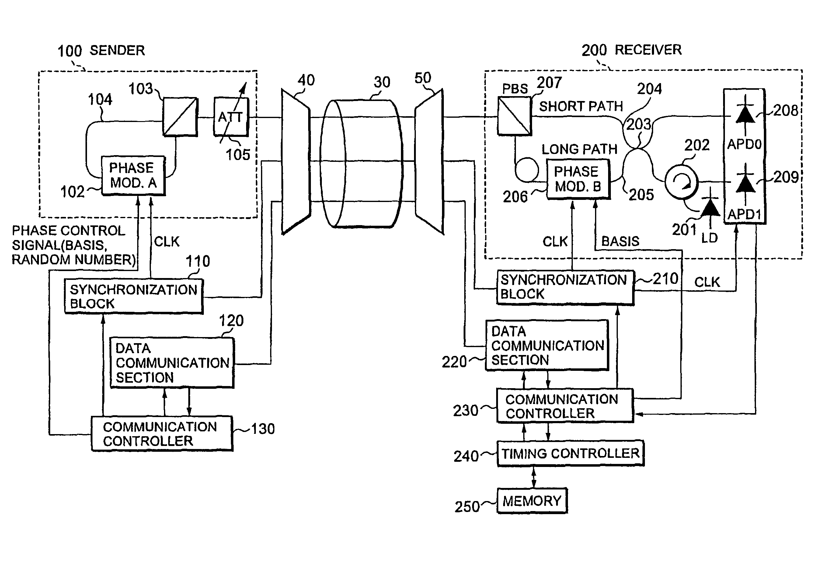
[0067]FIG. 3 is a block diagram showing a configuration of a temperature-independent plug and play system according to a first embodiment of the present invention. Note that blocks similar to those shown in FIG. 2 are given the same reference numerals and symbols as in FIG. 2. The basic configuration and operation of the plug and play system according to the present embodiment are as described in conjunction with FIG. 1, except that a PBS loop is employed in place of the faraday mirror in the sender.

[0068]The quantum block 100 in the sender 10 (here, Alice) has a PBS loop 104 and a variable optical attenuator 105. The PBS loop 104 includes a phase modulator 102 and a polarization beam splitter (PBS) 103.

[0069]The phase modulator 102 performs phase modulation on a sequence of optical pulses passing through itself, in accordance with a clock signal CLK supplied from the synchronization block 110. The depth of a phase modulation is determined by a phase control signa...

second embodiment

2. Second Embodiment

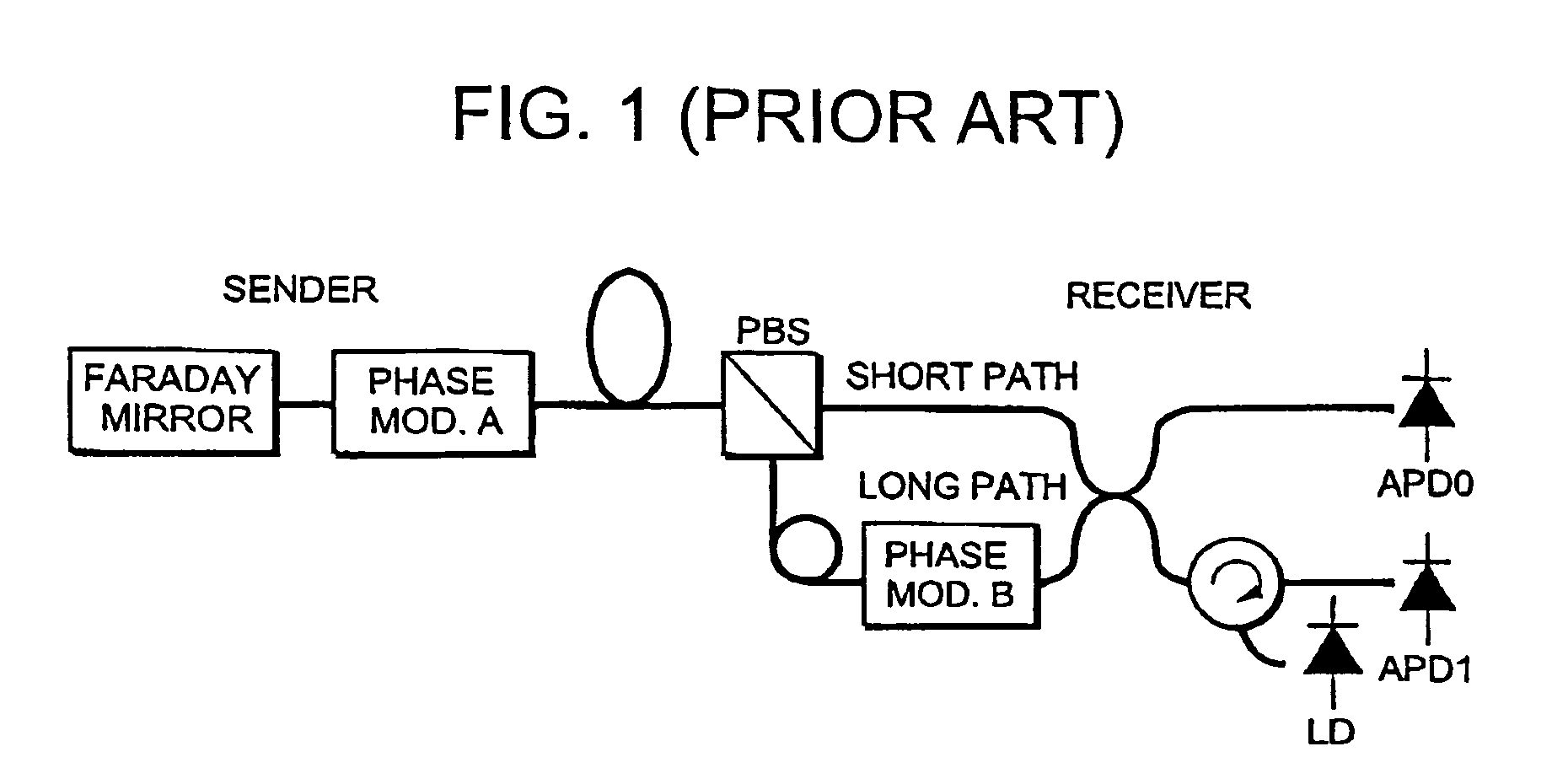
[0152]FIG. 16 is a block diagram showing a configuration of a quantum key distribution system according to a second embodiment of the present invention. As in the first embodiment, the quantum key distribution system according to the present embodiment employs a plug and play configuration. However, the present embodiment is different from the first embodiment in that a faraday mirror, not the PBS loop, is used in the quantum block 100 of the sender 10. Note that blocks having functions similar to those shown in FIG. 3 are given the same reference numerals and symbols as in FIG. 3, and detailed description thereof will be omitted.

[0153]The quantum block 100 in sender 10 includes a faraday mirror 101, phase modulator 102 and variable optical attenuator 105, which are connected in series. Double pulses coming from the transmission line 30 are reflected by the faraday mirror 101 with their polarization rotated by π / 2 each, and then the subsequent pulse only is modul...

fifth embodiment

4. Fifth Embodiment

[0219]4.1) Time-Direction Control of Timing Signal

[0220]FIG. 21 is a handshake diagram showing a procedure of the control of the sender's timing according to a fifth embodiment of the present invention, and FIG. 22 is a flowchart showing the procedure of the control of the sender's timing according to the fifth embodiment of the present invention. Control of the sender is all performed under instructions from the receiver. Since the phase modulator 102 in the sender is driven in accordance with a clock supplied from the synchronization block 110, the timing of driving the phase modulator 102 depends on the timing of supplying the clock (clock timing). The synchronization block 110 can shift the clock timing by an arbitrary number of steps ranging from 0 to 2π, under instructions from the communication controller 270 in the receiver.

[0221]First, the communication controller 270 in the receiver designates data “00” and notifies it to the sender (S801) and, through t...


PUM


Abstract

A communication system and a timing control method are proposed that optimize timing in a sender and thereby enable information to be stably transmitted at the right timing. Under instructions from a timing controller in a receiver, the timing of driving a phase modulator in a sender is shifted by one step after another, and the then amount of clock shift and result of interference are monitored at the receiver and stored in a memory. The optimum timing is determined based on the stored data. Thus, a clock for driving the phase modulator in the sender can be set at the right timing. This is equivalent to compensating for group velocity dispersion due to wavelength dispersion that occurs when an optical signal channel and a clock signal channel are transmitted by wavelength division multiplexing transmission.

Description

BACKGROUND OF THE INVENTION[0001]1. Field of the Invention[0002]The present invention relates to a communication system and, more particularly, to a system and method for determining the timing of an operation of a communication device.[0003]2. Description of the Related Art[0004]In recent years, in the field of optical communications, active studies have been devoted to quantum key distribution systems, which are expected to achieve high privacy levels over transmission links, and various proposals have been made.[0005]As a basic example, a system for sharing a quantum cryptographic key between a sender and a receiver by using two bases is proposed in Bennett and Brassard, “Quantum Cryptography: Public Key Distribution and Coin Tossing,” IEEE International Conference on Computers, Systems and Signal Processing, Bangalore, India, pp. 175-179. According to this proposal, a sender transmits single photons each modulated in phase with four types of information depending on the combinat...

Claims


Application Information

Patent Timeline
Patent Type & Authority Patents(United States)
IPC IPC(8): H04B10/04H04L7/00
CPCH04B10/548H04L9/0852
Inventor MAEDA, WAKAKOTAJIMA, AKIOTANAKA, AKIHIROTAKAHASHI, SEIGO
Owner NEC CORP
Why Eureka
Try Eureka