Resin encapsulated semiconductor device and method for manufacturing the same

a technology of encapsulation and semiconductors, applied in semiconductor devices, semiconductor/solid-state device details, electrical apparatus, etc., can solve the problems of increasing frequency demand, difficult to realize, and difficult to obtain high frequency characteristics sufficient to be used in high-frequency communications or the lik

Inactive Publication Date: 2012-06-05
TESSERA ADVANCED TECH
View PDF86 Cites 9 Cited by
  • Summary
  • Abstract
  • Description
  • Claims
  • Application Information

AI Technical Summary

Benefits of technology

[0044]According to this method, since in the step (a), the sealing tape is attached onto the lower surface of the lead frame, and the angle of the lower portion of the rising portion is sharp, the encapsulating resin can be prevented effectively from penetrating onto the lower surface of the external terminals in the step (c). In other words, this method makes it possible to manufacture a resin-encapsulated semiconductor device having no resin burr on the external terminal can be manufactured.

Problems solved by technology

However, the conventional structures require advanced processing techniques for the lead frame, which is the basic frame of a semiconductor device, in order to reduce the size of the resin-encapsulated semiconductor device and achieve higher density, so that it has been difficult to realize them.
On the other hand, in the structures of the conventional resin-encapsulated semiconductor devices, it is difficult to obtain high frequency characteristics sufficient to be used in high frequency communications or the like.
This is mainly because when high frequency signals are input to external terminals adjacent to each other of the resin-encapsulated semiconductor device, the high frequency signals interfere with each other, which causes noise.
For electronic components mounted in a set of equipment such as communication equipment, further higher frequencies are increasingly in demand, and the effects of the noise as described above become large.

Method used


Image

  • Resin encapsulated semiconductor device and method for manufacturing the same
  • Resin encapsulated semiconductor device and method for manufacturing the same
  • Resin encapsulated semiconductor device and method for manufacturing the same

Examples


first embodiment

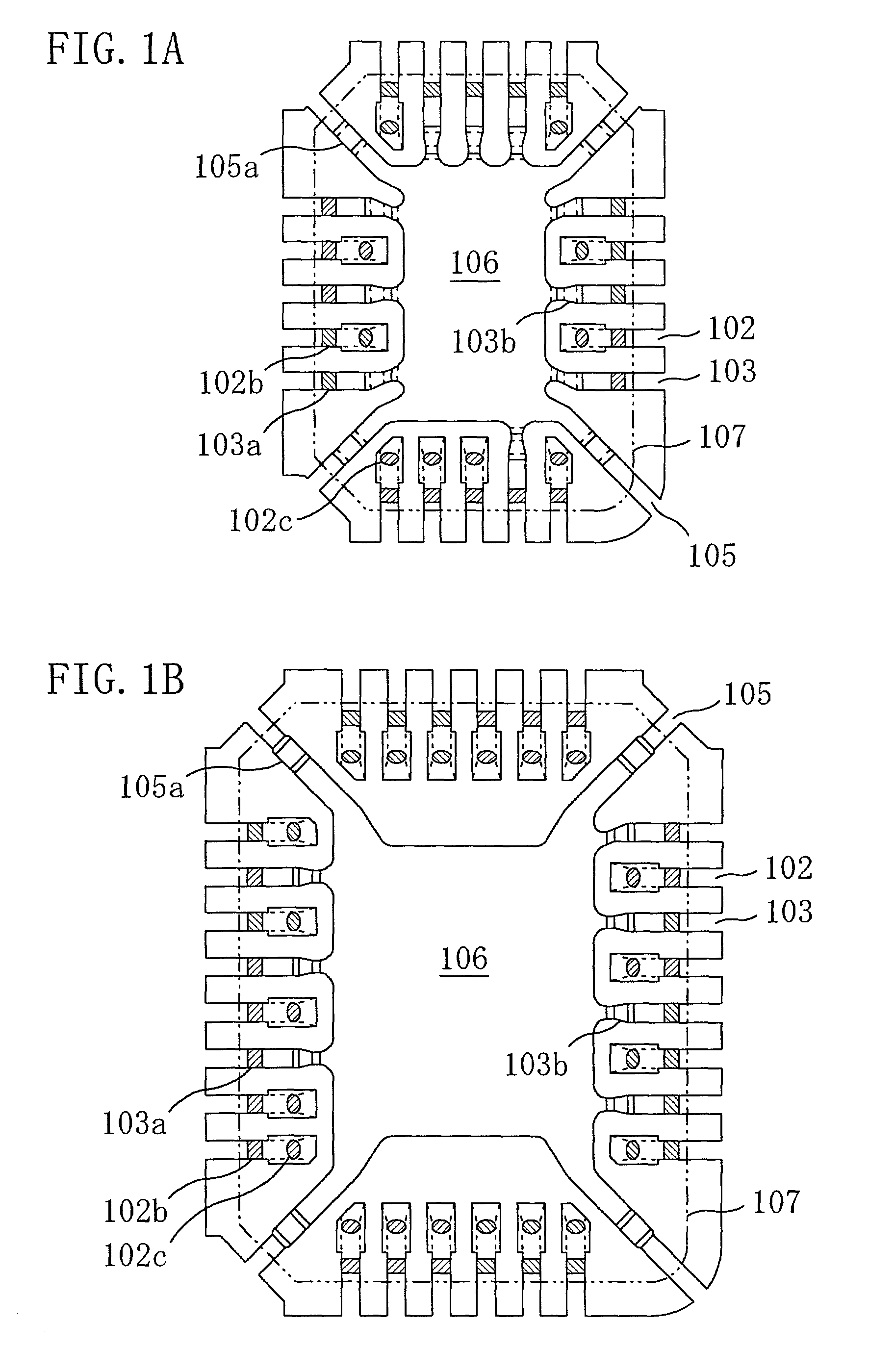
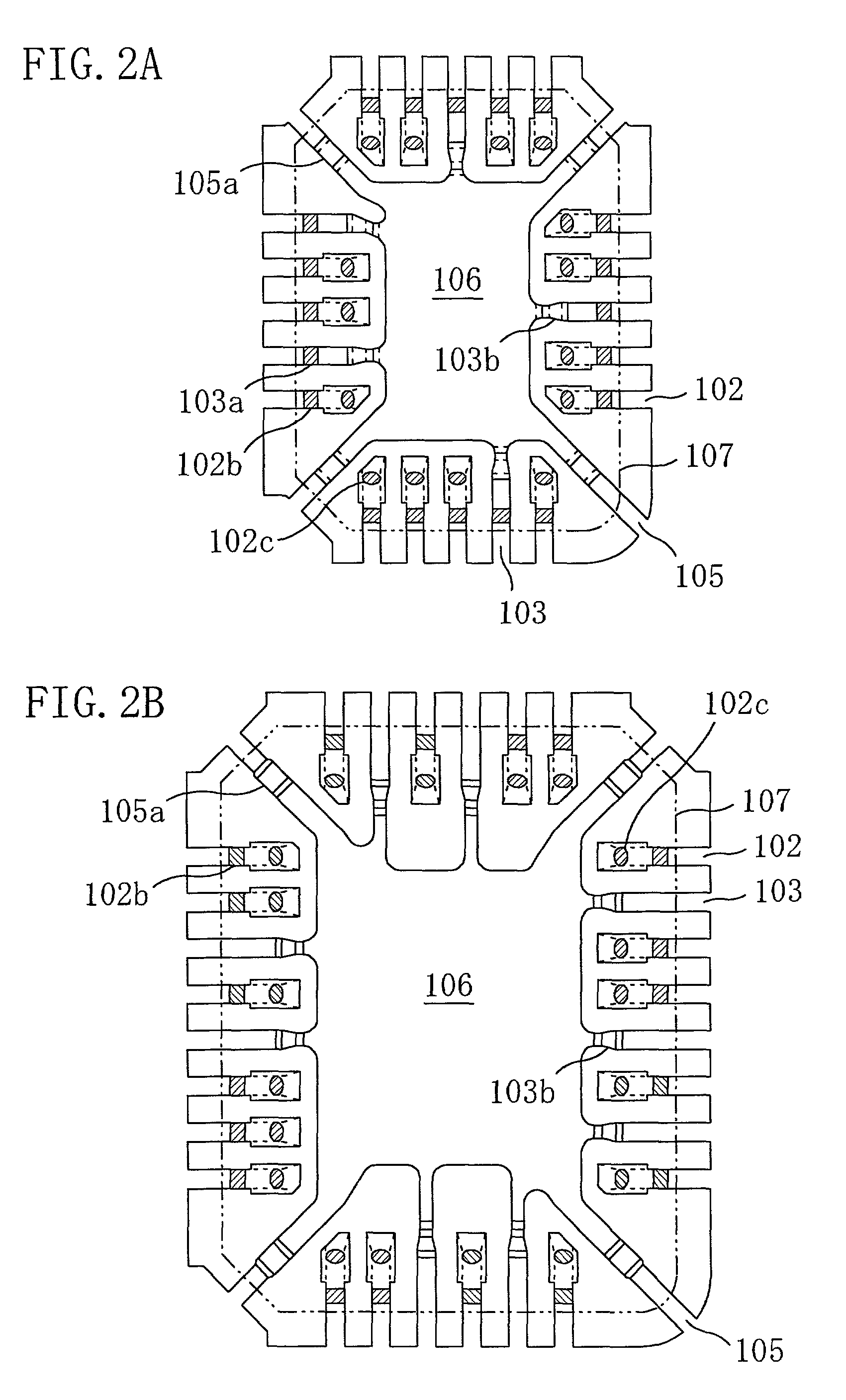
[0092]As a first embodiment of the present invention, a lead frame and a resin-encapsulated semiconductor device that is QFN manufactured with the lead frame will be described.

—Description of Lead Frame—

[0093]First, the lead frame used in the QFN resin-encapsulated semiconductor device of the first embodiment of the present invention (hereinafter, referred to as “the lead frame of this embodiment) will be described.

[0094]FIGS. 1A and 1B are views showing an example of the lead frame of this embodiment. As shown in FIG. 1A, within each framing portion, the lead frame of this embodiment includes a die pad 106 on which a semiconductor chip is to be mounted, suspended leads 105 for supporting the die pad 106, a plurality of signal leads 102 arranged around the die pad 106 that are connected to the framing portion, and ground connection leads 103 that are connected to the die pad 106 and the framing portion. The signal leads 102 have head grooves 102b and base grooves 102c.

[0095]These g...

second embodiment

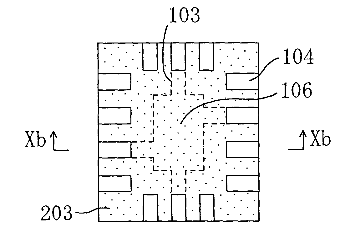
[0173]As a second embodiment of the present invention, HQFN (Quad Flat Non-leaded Package provided with a heat sink), which is a variation of the QFN, will be described.

[0174]FIGS. 27A to 27C are a plan view when viewed from the bottom, showing a resin-encapsulated semiconductor device of this embodiment that is HQFN, a cross-sectional view taken along XXVIIb-XXVIIb of the resin-encapsulated semiconductor device, and a cross-sectional view taken along XXVIIc-XXVIIc of the resin-encapsulated semiconductor device, respectively. As shown in FIGS. 27A to 27C, the resin-encapsulated semiconductor device of this embodiment are substantially a rectangular solid, and includes a die pad 126, a plurality of signal leads 122 provided along the four sides of the bottom surface of the device, ground connection leads 123 (not shown) connected to the die pad 126, a semiconductor chip 221 fixed on the upper surface of the die pad 126 with an adhesive and having electrode pads, and metal thin wires ...

third embodiment

[0195]As a third embodiment of the present invention, a resin-encapsulated semiconductor device that is an SON will be described with reference to the accompanying drawings.

[0196]FIG. 36A is a plan view when viewed from the bottom, showing a resin-encapsulated semiconductor device of this embodiment that is HSON (Small Outline Non-leaded Package provided with a heat sink). FIGS. 36B to 36D are cross-sectional views taken along line XXXVI-XXXVI of the resin-encapsulated semiconductor devices employing the lead frames that have been subjected to different processing. In the resin-encapsulated semiconductor device of this embodiment, the entire lower surface of the die pad is exposed, and even among the SONs, this device has the most improved heat release performance.

[0197]As shown in FIGS. 36A to 36D, the resin-encapsulated semiconductor device of this embodiment has a quadrangular bottom surface, and includes the die pad 136 whose lower surface is entirely exposed, the signal leads (...


PUM


Abstract

The present invention includes a die pad; signal leads, ground connection leads connected to the die pad; a semiconductor chip including electrode pads for grounding; metal thin wires, and an encapsulating resin for encapsulating the die pad and the semiconductor chip and encapsulating the signal leads and the ground connection lead such that lower portions of the signal leads and the ground connection lead are exposed as external terminals. The ground connection lead is connected to the electrode pad for grounding, so that the resin-encapsulated semiconductor device is electrically stabilized. Furthermore, interference between high frequency signals passing through the signal leads can be suppressed by the die pad and the ground connection leads.

Description

BACKGROUND OF THE INVENTION[0001]The present invention relates to a lead frame, a method for manufacturing the same, a resin-encapsulated semiconductor device in which the lead frame and a semiconductor chip are encapsulated with resin, and a method for manufacturing the same. In particular, the present invention relates to a resin-encapsulated semiconductor device manufactured to achieve electrical stability and to improve the high frequency characteristics, a method for manufacturing the same, a lead frame used in the resin-encapsulated semiconductor device, and a method for manufacturing the same.[0002]In recent years, in response to compactness and high density of electronic equipment, there is an demand for high density and high performance of semiconductor components such as resin-encapsulated semiconductor devices, and this trend has promoted the development of more compact and thinner semiconductor components. In this context, a semiconductor device called QFP (Quad Flat Pac...

Claims


Application Information

Patent Timeline
Patent Type & Authority Patents(United States)
IPC IPC(8): H01L23/495H01L23/28H01L21/48H01L21/56H01L23/12H01L23/31H01L23/50
CPCH01L21/4842H01L23/3107H01L23/49503H01L23/49548H01L24/97H01L21/565H01L24/49H01L2224/92247H01L2224/32014H01L2224/48091H01L2224/48137H01L2224/48247H01L2224/48465H01L2224/48471H01L2224/49113H01L2224/4912H01L2224/4917H01L2224/49171H01L2224/49175H01L2224/4945H01L2224/73265H01L2224/81005H01L2224/85191H01L2224/97H01L2924/01004H01L2924/01013H01L2924/01029H01L2924/01032H01L2924/01033H01L2924/01046H01L2924/01047H01L2924/01078H01L2924/01079H01L2924/01082H01L2924/10329H01L2924/18301H01L2924/30105H01L2924/30107H01L2924/3011H01L2924/01006H01L2924/01005H01L2224/32245H01L24/48H01L2224/85H01L2924/00014H01L2924/00H01L2924/00012H01L2224/48227H01L2224/451H01L2224/45015H01L2924/181H01L24/45H01L2224/48257H01L2224/05554H01L2224/05553H01L2224/06179H01L2224/49111H01L2224/49433H01L24/06H01L2224/0603H01L2924/10161H01L2924/20752H01L2924/00015H01L2924/20753H01L2224/05599H01L2224/4554H01L23/495
Inventor KAWAI, FUMIHIKOFUKUDA, TOSHIYUKIMINAMIO, MASANORITAKEUCHI, NOBORUOGATA, SHUICHITARA, KATSUSHINAKATSUKA, TADAYOSHI
Owner TESSERA ADVANCED TECH
Why Eureka
Try Eureka