Multichannel interfacing device having a termination circuit

a multi-channel interfacing and termination circuit technology, applied in the direction of logic circuit coupling/interface arrangement, line-transmission details, pulse technique, etc., can solve the problems of scheme being vulnerable to external crosstalk, method subject to two detrimental phenomena, and generating nois

Inactive Publication Date: 2012-07-17
ZXNOISE LLC
View PDF15 Cites 221 Cited by
  • Summary
  • Abstract
  • Description
  • Claims
  • Application Information

AI Technical Summary

Benefits of technology

[0043]According to the invention, the termination circuit in the activated state may be such that each diagonal component of said wanted non-diagonal matrix of size m×m has, in said part of said known frequency band, an absolute value less than or equal to thousand ohms and a real part greater than or equal to three ohms and greater than or equal to one tenth of said absolute value. Experience shows that the set of the dynamic impedances defined by these inequalities contains the impedance values capable of effectively reducing the reflections of signals propagating through typical interconnections.
[0056]A device of the invention may be such that it constitutes a part of an integrated circuit, each of said m signal terminals being coupled to one or more pins of said integrated circuit, said common terminal being coupled to one or more pins of said integrated circuit. This configuration is appropriate when said interconnection is realized outside said integrated circuit. The specialist notes that if there are many signal terminals, for instance more than 16 signal terminals, the absolute value of the current which may flow through the common terminal may become much larger than the maximum absolute value of the current flowing through a single signal terminal. Consequently, in this case, if a single pin is allocated to the common terminal, a degradation of transmission may occur for fast signals, because of the inductance of a connection using a single pin. In this case, using several pins for the common terminal reduces this inductance and improves transmission.

Problems solved by technology

This method is subject to two detrimental phenomena: echo and crosstalk between the different transmission channels.
However, there are other crosstalk phenomena which may produce noise.
This scheme is consequently vulnerable to external crosstalk (it is also subject to internal crosstalk).
Unfortunately, the termination circuit (4) shown in FIG. 2 produces return currents flowing mainly in the reference conductor, a characteristic which conflicts with the reduction of external crosstalk.
Unfortunately, the termination circuit (4) shown in FIG. 3 produces return currents flowing mainly in the reference conductor, a characteristic which conflicts with the reduction of external crosstalk.
However, it does not eliminate internal crosstalk.

Method used


Image

  • Multichannel interfacing device having a termination circuit
  • Multichannel interfacing device having a termination circuit
  • Multichannel interfacing device having a termination circuit

Examples


first embodiment

Best Mode

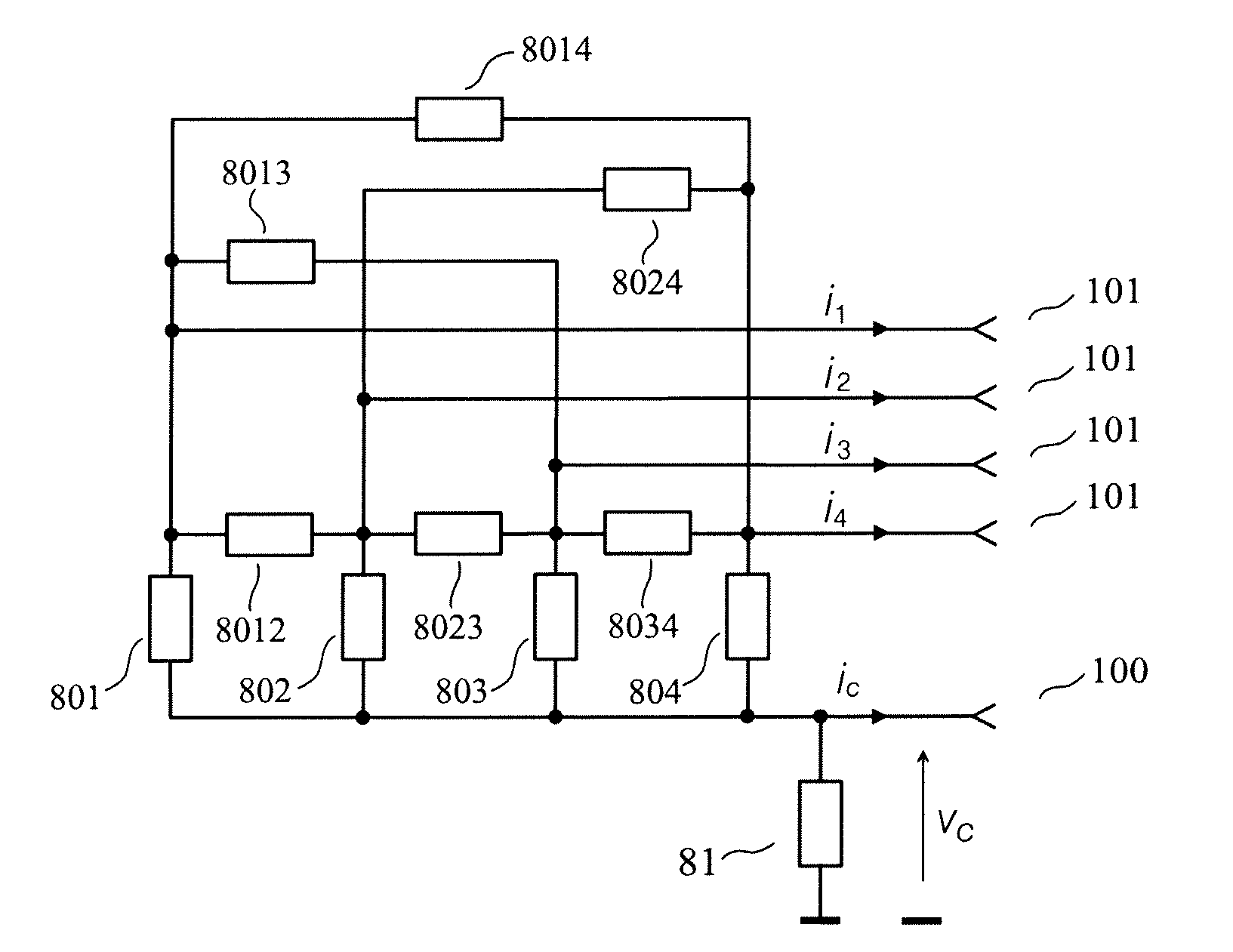
[0083]As a first embodiment of an interfacing device of the invention, given by way of non-limiting example and best mode of carrying out the invention, we have represented in FIG. 8 an interfacing device of the invention built inside an integrated circuit, comprising m=4 signal terminals (101) and a common terminal (100), the signal terminals (101) and the common terminal (100) being intended to be connected to an interconnection having m=4 transmission conductors. The signal terminals (101) are numbered from 1 to m.

[0084]A receiving circuit (6) delivers, when the receiving circuit is in the activated state, p=4 “output signals of the receiving circuit” corresponding each to a transmission channel, the input of the receiving circuit being coupled to the 4 signal terminals (101) and to the common terminal (100), each of said “output signals of the receiving circuit” being determined by a linear combination of the voltages between one of said signal terminals (101) and said ...

second embodiment

[0093]As a second embodiment of an interfacing device of the invention, given by way of non-limiting example, we have represented in FIG. 11 an interfacing device of the invention comprising m=4 signal terminals (101) and a common terminal (100), the signal terminals (101) and the common terminal (100) being intended to be connected to an interconnection having m=4 transmission conductors.

[0094]A transmitting circuit (5) receives q=4 “input signals of the transmitting circuit” coming from a source (2), the output of the transmitting circuit being coupled to the 4 signal terminals (101). The output of the transmitting circuit (5) delivers, when the transmitting circuit is in the activated state, q=4 transmission variables, each transmission variable being a current flowing out of one of said signal terminals (101), each transmission variable being mainly determined by a linear combination of said “input signals of the transmitting circuit”. When the transmitting circuit (5) is not in...

third embodiment

[0109]The third embodiment of an interfacing device of the invention, given by way of non-limiting example, is shown in FIG. 13. The receiving circuit (6) and the termination circuit (4) shown in FIG. 13 are such that:

[0110]each of the p=3 “output signals of the receiving circuit” is delivered to an output (68) which is a differential output comprising 2 terminals (681) (682);

[0111]each of the p outputs (68) corresponds to the output of a differential pair made of two transistors (611) (612) whose sources are biased by a current source (613) and whose drains are biased by two resistors (631) (632);

[0112]each of the m=3 signal terminals (101) is connected to the gate of the first transistor (611) of one of said differential pairs;

[0113]the common terminal (100) is connected to the gates of the p second transistors (612) of said differential pairs;

[0114]the termination circuit (4) is made of m resistors (431) connected between one of said signal terminals (101) and said common termina...


PUM


Abstract

The invention relates to an interfacing device for transmission through interconnections used for sending a plurality of electrical signals.The interfacing device of the invention comprises signal terminals and a common terminal. A receiving circuit delivers, when the receiving circuit is in the activated state, “output signals of the receiving circuit” determined each by a linear combination of the voltages between one of the signal terminals and the common terminal, to the destination. A termination circuit is such that, when it is in the activated state, it is approximately equivalent, for the signal terminals and the common terminal, to a (m+1)-terminal network such that, for small signals, the impedance matrix, with respect to the common terminal, of the (m+1)-terminal network is equal to a wanted non-diagonal matrix of size m×m.

Description

CROSS REFERENCE TO RELATED APPLICATIONS[0001]This is a Continuation Application of PCT application PCT / IB2009 / 051182, filed 20 Mar. 2009, published in English under No. WO 2010 / 004444, which in turn claims priority to French patent application number 08 / 03876 of 8 Jul. 2008, entitled “Dispositif d'interface multicanal avec circuit de terminaison”, both of which are incorporated herein by reference.FIELD OF THE INVENTION[0002]The invention relates to an interfacing device for transmission through interconnections used for sending a plurality of electrical signals, such as the interconnections made with multiconductor cables, or with the traces of a printed circuit board, or inside an integrated circuit.PRIOR ART[0003]Let us consider the problem of transmission through an interconnection, for obtaining m transmission channels, m being an integer greater than or equal to 2. Each transmission channel may be used for transmitting signals of any type, for instance analog signals or digita...

Claims


Application Information

Patent Timeline
Patent Type & Authority Patents(United States)
IPC IPC(8): H03K17/16
CPCH04B3/30H04L25/0272H04L25/0298
Inventor BROYDE, FREDERICCLAVELIER, EVELYNE
Owner ZXNOISE LLC
Why Eureka
Try Eureka