Method for via stub elimination

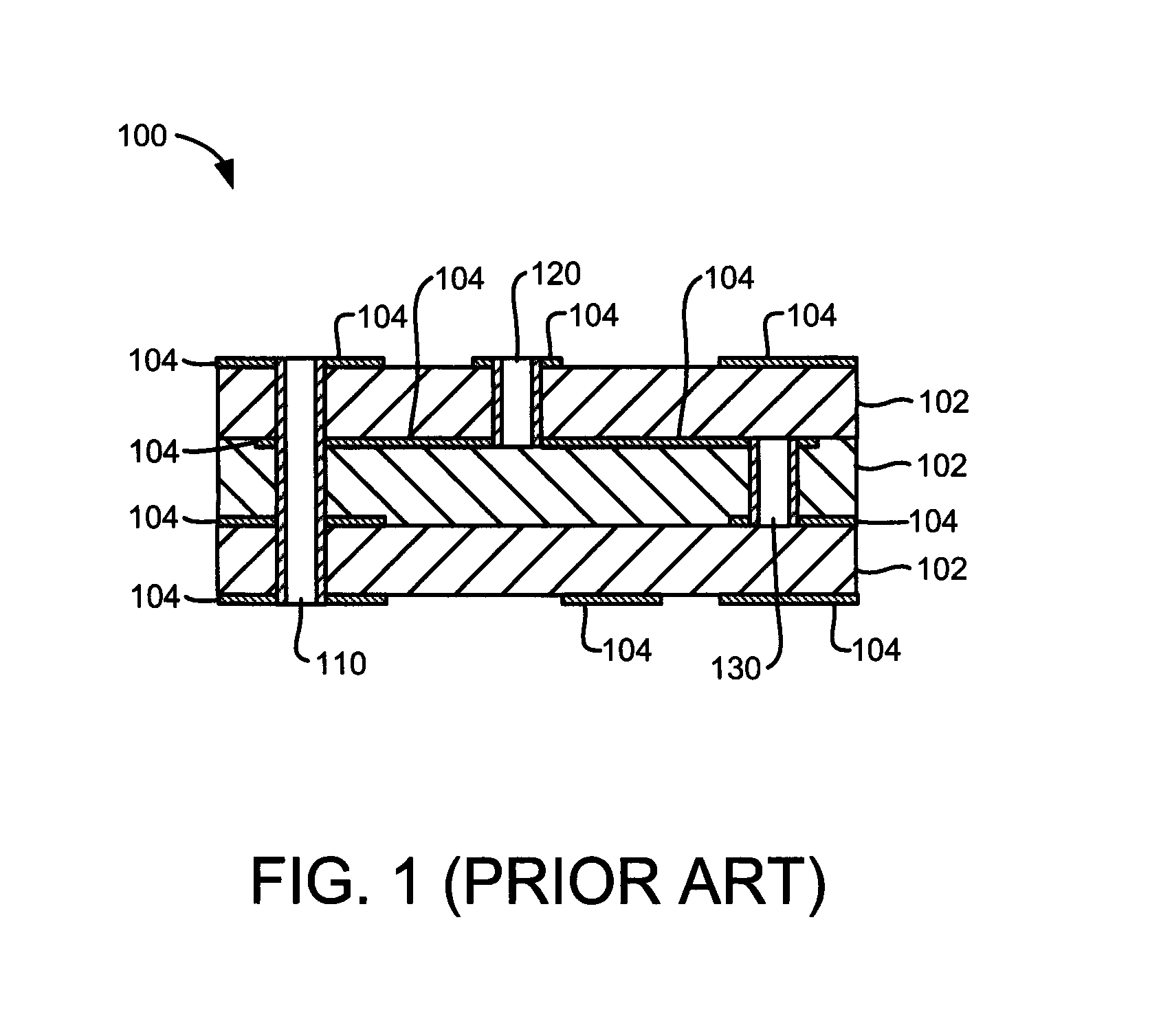
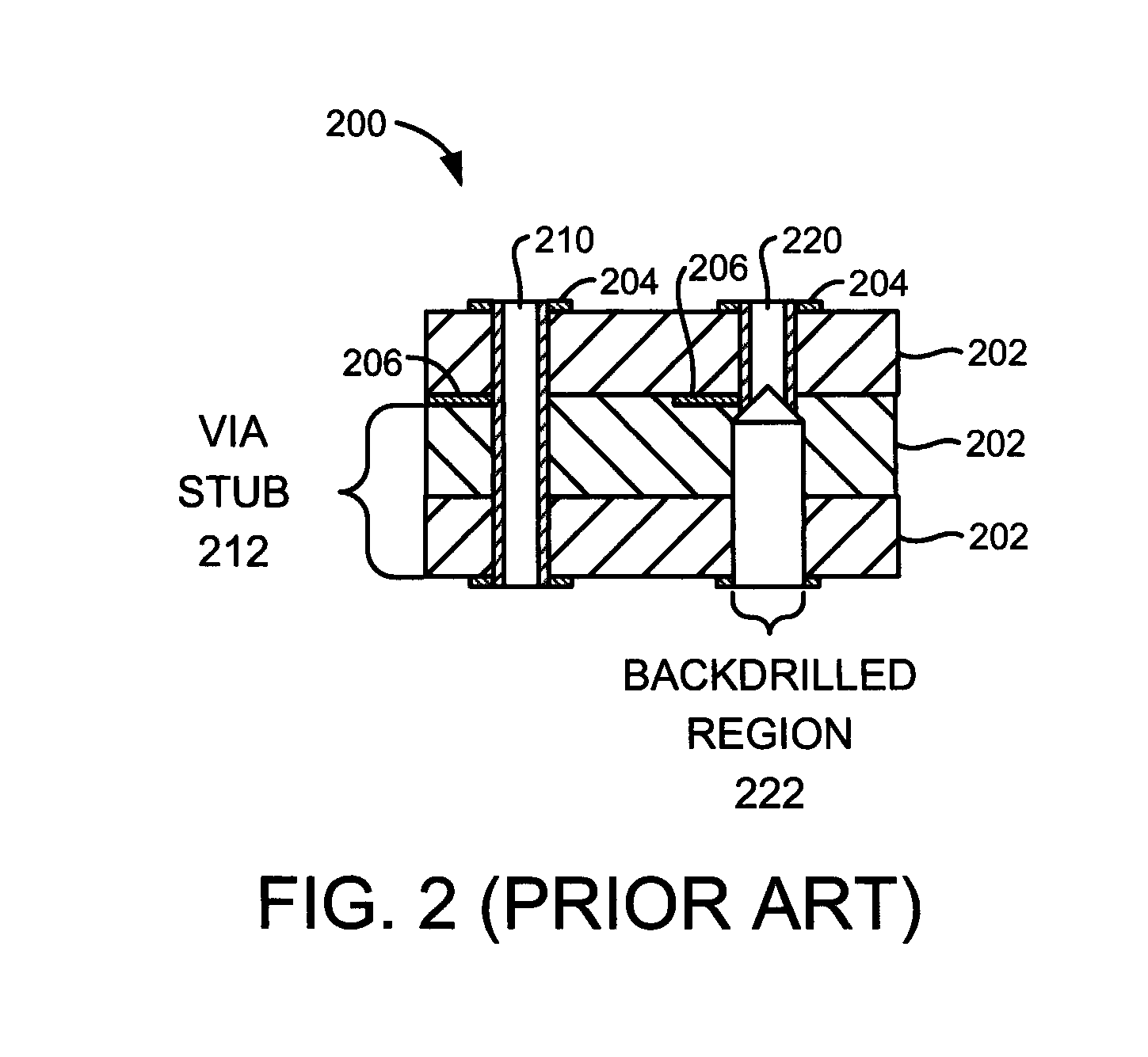
a technology of backdrilling and vias, applied in the field of electric connectors, can solve the problems of high cost of fabricating blind vias and buried vias, time-consuming and labor-intensive backdrilling, etc., and achieve the effect of eliminating the cost and time-consuming process of backdrilling vias

Inactive Publication Date: 2012-07-31
GLOBALFOUNDRIES INC
View PDF9 Cites 9 Cited by
  • Summary
  • Abstract
  • Description
  • Claims
  • Application Information

AI Technical Summary

Benefits of technology

[0010]According to the preferred embodiments of the present invention, a substrate (e.g. a printed wiring board or other substrate, such as an interconnect substrate) includes a plurality of insulator layers and internal conductive traces. First and second through-holes extend completely through the substrate and respectively pass through first and second ones of the internal conductive traces, which are at different depths within the substrate. Photolithographic techniques are used to generate plated-through-hole (PTH) plugs of controlled, variable depth in the through-holes before first and second conductive vias are respectively plated onto the first and second through-holes. The depth of these PTH plugs is controlled (e.g., using a photomask and / or variable laser power) to prevent the first and second conductive vias from extending substantially beyond the first and second internal conductive traces, respectively, and thereby prevent via stubs from being formed in the first place. This advantageously eliminates the costly and time consuming process of via stub backdrilling.

Problems solved by technology

However, blind vias and buried vias are significantly more expensive to fabricate than PTH vias because blind vias and buried vias are produced utilizing additional fabrication steps that are performed as the insulator layers of the PWB are fabricated.
Unfortunately, backdrilling is a costly, time-consuming process.

Method used


Image

  • Method for via stub elimination
  • Method for via stub elimination
  • Method for via stub elimination

Examples


Embodiment Construction
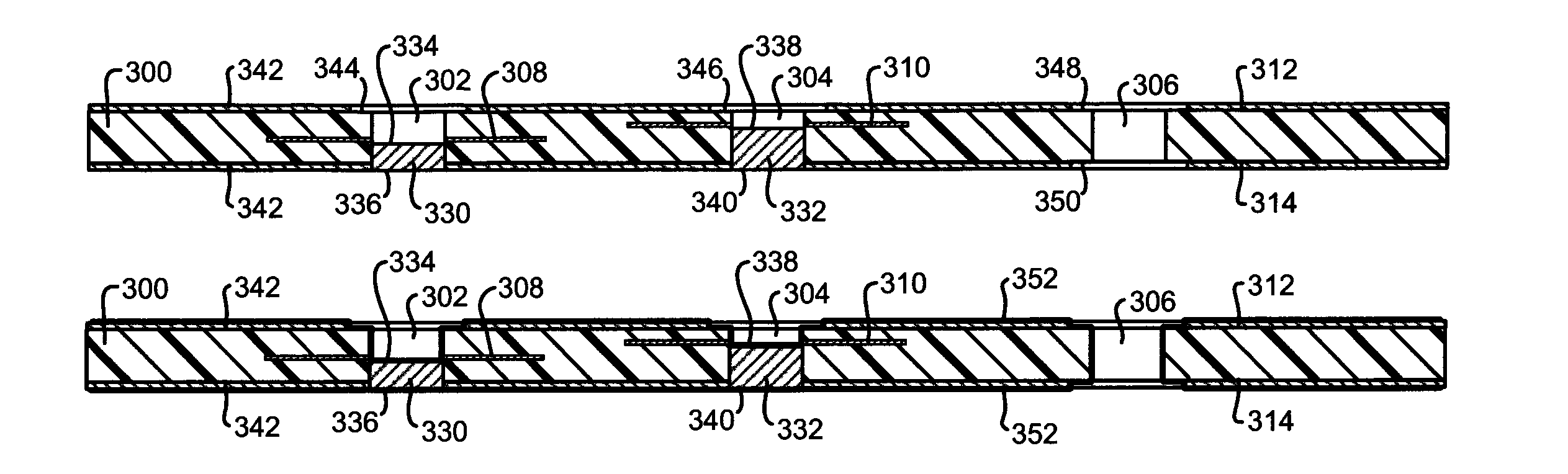
[0032]1.0 Overview

[0033]In accordance with the preferred embodiments of the present invention, a substrate (e.g. a printed wiring board or other substrate, such as an interconnect substrate) includes a plurality of insulator layers and internal conductive traces. First and second through-holes extend completely through the substrate and respectively pass through first and second ones of the internal conductive traces, which are at different depths within the substrate. Photolithographic techniques are used to generate plated-through-hole (PTH) plugs of controlled, variable depth in the through-holes before first and second conductive vias are respectively plated onto the first and second through-holes. The depth of these PTH plugs is controlled to prevent the first and second conductive vias from extending substantially beyond the first and second internal conductive traces, respectively, and thereby prevent via stubs from being formed in the first place. This advantageously elimina...


PUM

PropertyMeasurementUnit
conductiveaaaaaaaaaa
neutral densityaaaaaaaaaa
poweraaaaaaaaaa

Abstract

An enhanced mechanism is disclosed for via stub elimination in printed wiring boards (PWBs) and other substrates. In one embodiment, the substrate includes a plurality of insulator layers and internal conductive traces. First and second through-holes extend completely through the substrate and respectively pass through first and second ones of the internal conductive traces, which are at different depths within the substrate. Photolithographic techniques are used to generate plated-through-hole (PTH) plugs of controlled, variable depth in the through-holes before first and second conductive vias are respectively plated onto the first and second through-holes. The depth of these PTH plugs is controlled (e.g., using a photomask and / or variable laser power) to prevent the first and second conductive vias from extending substantially beyond the first and second internal conductive traces, respectively, and thereby prevent via stubs from being formed in the first place. This advantageously eliminates the costly and time consuming process of via stub backdrilling.

Description

CROSS-REFERENCE TO RELATED APPLICATION[0001]This patent application is related to pending U.S. patent application Ser. No. 12 / 193,842, filed concurrently, entitled “HORIZONTALLY SPLIT VIAS”, which is assigned to the assignee of the instant application, and which is incorporated herein by reference in its entirety.BACKGROUND OF THE INVENTION[0002]1. Field of Invention[0003]The present invention relates in general to the electrical connector field. More particularly, the present invention relates to a method and apparatus for eliminating a via stub in printed wiring boards (PWBs) and other substrates, such as interconnect substrates.[0004]2. Background Art[0005]Electrical connectors are in widespread use in the electronics industry. In many computer and other electronic circuit structures, an electronic module such as a central processor unit (CPU), memory module, application-specific integrated circuit (ASIC) or other integrated circuit, must be connected to a printed wiring board (P...

Claims


Application Information

Patent Timeline
Patent Type & Authority Patents(United States)
IPC IPC(8): H01K3/10
CPCH05K1/115H05K3/429H05K1/0237H05K3/0082H05K3/184H05K3/422Y10T29/49155H05K2203/056H05K2203/0565Y10T29/4913Y10T29/49126Y10T29/49165H05K2201/09645B33Y80/00
Inventor KUCZYNSKI, JOSEPHSPLITTSTOESSER, KEVIN ALBERTTOFIL, TIMOTHY JEROMEVERMILYEA, PAUL ALAN
Owner GLOBALFOUNDRIES INC
Why Eureka
Try Eureka