Thermionic electron emitter and X-ray source including same

a technology of electron emitter and x-ray source, which is applied in the direction of discharge tube/lamp details, x-ray tube main electrode, discharge tube/lamp details, etc., can solve the problems of significant negative change in the intensity distribution and optical quality of the focal spot system, and inability to stabilize the mechanical connection between the external segments, etc., to achieve minimal focal spot size, minimal response time, and superior properties

Inactive Publication Date: 2012-08-28
KONINK PHILIPS ELECTRONICS NV
View PDF7 Cites 13 Cited by
  • Summary
  • Abstract
  • Description
  • Claims
  • Application Information

AI Technical Summary

Benefits of technology

[0026]According to an embodiment of the invention, the surrounding surface, in the isolation region, is laterally spaced apart from the emission surface by a gap. This gap may serve for thermal isolation. For example, this gap may have a width of less than 1 mm, preferably less than 0.4 mm and more preferably less than 0.2 mm. The smaller the gap the smaller disturbances of the electrical field may be. Preferably, the gap may have a constant width along its longitudinal extension in order to reduce inhomogeneities in electric field deviations and / or thermal properties.
[0027]According to a further embodiment, the heating arrangement comprises two emitter terminals arranged at the inner part at opposing positions with respect to the emission surface such that an electrical heating current can be induced in the emission surface by applying a voltage to the emitter terminals. In this embodiment, the emission surface can be directly heated. The location at which the emitter terminals contact the inner part of the electron emitter may define the lateral extremities of the heatable emission surface. Due to radiation losses, conduction losses and convection losses, these extremities may be the coldest areas of the heated emission surface. Accordingly, it may be advantageous to mechanically connect the unheated outer part to the inner part at proximity to these extremities.
[0030]According to a further embodiment of the electron emitter the inner part and the outer part are integrally formed from the same material such as for example a metal, a metal alloy or a metal sandwich combination. Suitable materials can be for example tungsten, tantalum and tungsten rhenium alloy. Forming the inner part and the outer part integrally from a common substrate may at the same time improve producibility and mechanical stability of the electron emitter. Furthermore, as the entire electron emitter is formed from an electrically conductive material, the inner part and the outer part are in electrical connection. Furthermore, being of the same material, all parts of the electron emitter have the same coefficient of expansion which may be advantageous in high temperature environments.
[0032]According to a further embodiment, the emission surface of the inner part and the surrounding surface of the outer part are arranged in a same plane. In such arrangement, the electron emitter can be fabricated for example from a simple flat film or sheet substrate wherein the surrounding surface is separated from the heatable emission surface only by small slits or gaps which may be fabricated for example by lasering or wire erosion. The thickness of such sheet may be for example in the range of a few hundred micrometers. Having a completely flat surface including the emission surface and the surrounding surface, an electron emitter according to this embodiment may be advantageous in order to obtain an undistorted electrical field between the emission surface and a remote anode.
[0033]According to a further embodiment, the surrounding surface extends out of the plane of the emission surface. For example, the surrounding surface can be laterally continuous to the emission surface in a region directly adjacent to the emission surface but then bent out of the plane of the emission surface. Alternatively, the outer part including the surrounding surface can for example be attached on top of the border region of the inner part such that the surrounding surface extends in a plane parallel to the plane of the emission surface. Such different geometries of the surrounding surface may allow different electron-optical behaviours of the electron emitter.
[0034]According to a second aspect of the invention, an X-ray source including a thermionic electron emitter as described above is provided. Due to the advantageous properties of the thermionic electron emitter such as homogeneous electron emission, the X-ray source may reveal superior properties with respect to X-ray beam homogeneity, achievable tube current, achievable minimal focal spot size and achievable minimal response time. Apart from the inventive electron emitter, the X-ray source may comprise an anode to establish an electrical field between the electron emitter serving as a cathode and a target for generating the X-ray beam. Furthermore, electron optics may be provided.

Problems solved by technology

Accordingly, the electron emission characteristics may be drastically disturbed which also may cause a significant negative change in the focal spot intensity distribution and optical quality of the X-ray system.
However, such reduced web size may result in a mechanical connection between the external segments 309 and the emission surface 303 being not stable under external forces like the centrifugal force on CT-gantries any more.
Furthermore, any kind of slits within or close to the emission surface 303 of the emitter may lead to deformations in the high voltage field which may result in larger focal spot sizes.

Method used


Image

  • Thermionic electron emitter and X-ray source including same
  • Thermionic electron emitter and X-ray source including same
  • Thermionic electron emitter and X-ray source including same

Examples


Embodiment Construction

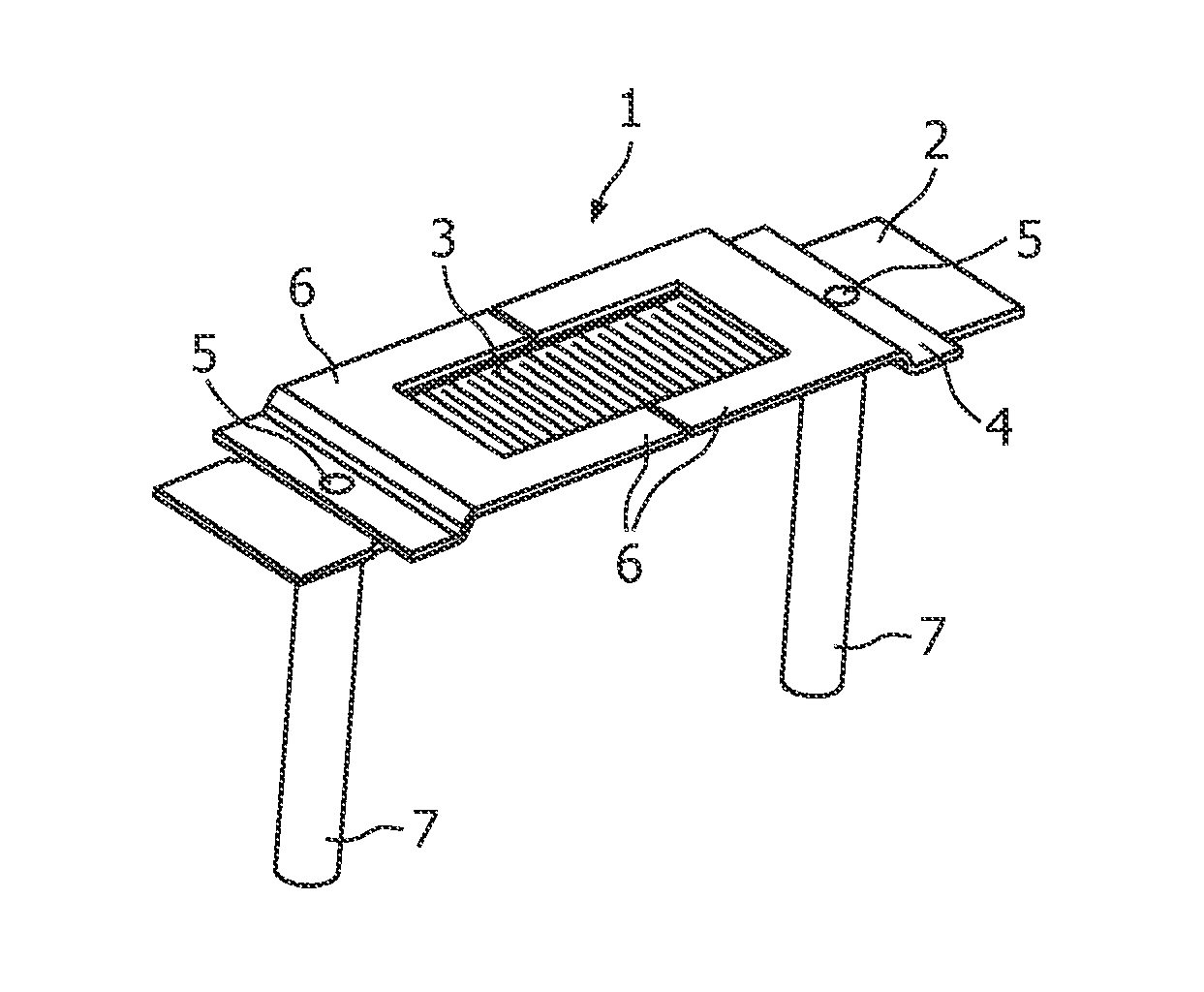
[0051]FIG. 6 shows a top view of a thermionic electron emitter 1 according to a first embodiment of the invention. The electron emitter 1 comprises an inner part 2 and an outer part 4 substantially enclosing the inner part 2. On the inner part 2, connection points 5 are provided which are to be connected with terminals for applying an external voltage to a region between lateral extremities of the inner part, this intermediate region serving as heatable flat emission surface 3.

[0052]In the drawing, the emission surface 3 is shown with different hatchings wherein a dense hatching indicates a higher temperature during operation when a current is flowing through the emission surface whereas a less dense hatching indicates a lower temperature during operation. It can be seen that at the centre between the two connection points 5 there is the highest temperature whereas in the border regions the temperature remains lower.

[0053]Accordingly, the terminals connected to the connection points...


PUM


Abstract

A thermionic electron emitter (1) is proposed comprising an inner part (2) including a heatable flat emission surface (3) and an outer part (4) including a surrounding surface (6) substantially enclosing the emission surface and a heating arrangement for heating the emission surface to a temperature for thermionic electron emission. The outer part is mechanically connected to the inner part in a connection region (10) apart from the emission surface. Furthermore, the surrounding surface is thermally isolated, e.g. by a gap (14), from the emission surface in an isolation region apart from the connection region. By providing a surrounding surface enclosing the emission surface which may be on a similar electrical potential as the emission surface but which can have a substantially lower temperature than the emission surface without influencing the temperature distribution within the emission surface, an improved electron emission distribution and homogeneity can be obtained.

Description

FIELD OF THE INVENTION[0001]The present invention relates to a thermionic electron emitter for emitting electrons by thermionic emission and an X-ray source including such thermionic electron emitter.TECHNICAL BACKGROUND[0002]Future demands for high-end CT (computer tomography) and CV (cardio vascular) imaging regarding the X-ray source are higher power / tube current, shorter response-times regarding the tube current, especially when pulse modulation is desired, and smaller focus spots corresponding to the demands of future detector systems.[0003]One key to reach higher power in smaller focus spots may be given by using a sophisticated electron-optical concept. But of the same importance may be the electron source itself and the starting conditions of the electrons. For a thermionic electron emitter for X-ray tubes it may be essential to heat up a metal surface to get electron emission currents of up to 1-2 A. These electron currents within the tube may be necessary for state-of-the-...

Claims


Application Information

Patent Timeline
Patent Type & Authority Patents(United States)
IPC IPC(8): H01J35/06
CPCH01J1/13H01J35/06H01J35/064
Inventor HAUTTMANN, STEFAN
Owner KONINK PHILIPS ELECTRONICS NV
Why Eureka
Try Eureka