Method of processing signal data with corrected clock phase offset

a clock phase offset and signal data technology, applied in the field of processing signal data, can solve the problems of more significant parameters, more involved clock distribution, and increased mismatch between different clock buffers or different clock paths, so as to achieve accurate signal data processing

Active Publication Date: 2012-09-04
INTEGRATED DEVICE TECH INC
View PDF67 Cites 23 Cited by
  • Summary
  • Abstract
  • Description
  • Claims
  • Application Information

AI Technical Summary

Benefits of technology

[0026]Whilst static offset can be corrected for by initial calibration, dynamic clock offsets which evolve during use of a signal data processing apparatus cannot. The present technique recognises and addresses this by continuously measuring the phase difference between the first and second clock signals and adjusting the current phase offset of at least one of those clock signals in dependence of the measured phase difference. In this way a target phase difference between the clock signals can be maintained, despite the evolution of dynamic clock offsets during the operation of the signal data processing apparatus. Hence account may be made for both static and dynamic sources of clock phase offset. Not only may initial clock offsets be calibrated for, but clock phase offset is monitored and corrected for in real time.
[0036]In the situation where the signal data is received signal data, the received signal data may have a clock signal embedded in it and in one embodiment the first clock signal and / or second clock signal are aligned with a recovered clock signal recovered from the received signal data. It will be recognised that this alignment assists in the accurate signal data processing of that received signal data.
[0037]Whilst in some embodiments a phase control signal may be generated for each measured phase difference, in one embodiment generating said at least one phase control signal is performed in dependence upon a plurality of measured phase differences. In this way variations over time may be monitored and appropriately responded to.

Problems solved by technology

As signal data processors become ever smaller (due to process shrinking) and more complex, this parameter becomes a more significant problem faced by the designers of such signal data processors.
Firstly as complementary metal-oxide-semiconductor (CMOS) minimum feature sizes become smaller, the mismatch between different clock buffers or different clock paths increases dramatically.
Secondly, due to the increased complexity of mixed signal circuit (high speed PHY) designs, clock distribution becomes more involved.
Clocks need more buffers or more complicated clock trees to be delivered to their destinations, which increases the clock delay mismatch significantly.
Thirdly, higher data and clock rates make the situation even worse even with the same ΔTd design.
Such factors become more significant as geometries decrease and may cause the clock offset to vary.
Such dynamic variation in the clock offset can lead to levels of jitter that are problematic when signal data processing.
Because of this iclk and qclk not only suffer from static clock offset (e.g delay mismatch), but may also suffer from dynamically evolving clock offsets (e.g due to INL, temperature dependent delay mismatch or power supply dependent mismatch).
The latter dynamic clock offsets are not addressed by power up reset or initial calibration, and as application speeds increase and process geometries decrease dynamic offset becomes one of the most significant limiting factors on coping with variations in clock phase offsets.

Method used


Image

  • Method of processing signal data with corrected clock phase offset
  • Method of processing signal data with corrected clock phase offset
  • Method of processing signal data with corrected clock phase offset

Examples


Embodiment Construction

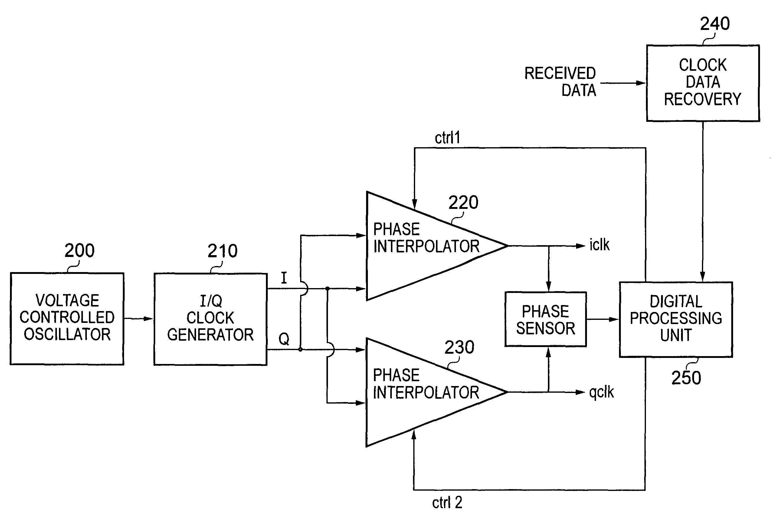
[0057]FIG. 4 schematically illustrates a first example embodiment of the present invention in which a receiver generates two clock signals aligned with the clock signal in a received data stream. Voltage control oscillator (VCO) 200 generates a single frequency clock locked to a reference clock. This single frequency clock is passed to I / Q clock generation block 210 which creates two clocks with 90 degree offset from one another (I-clock and Q-clock). Note that in other embodiments it is also possible for the VCO to generate the I / Q clocks directly. The I and Q clocks are then passed to phase interpolators (PIs) 220 and 230. From these inputs the two PIs create two new clocks, iclk and qclk, with 90 degree offset from one another, as well as aligned with the clock signal in the received data. The iclk and qclk clocks are then used to sample and recover incoming data.

[0058]The alignment of iclk and qclk with the clock signal in the received data occurs by means of clock data recovery...


PUM


Abstract

The present invention provides a method of processing signal data comprising generating a first clock signal and a second clock signal and processing the signal data using the first clock signal and the second clock signal. While processing the signal data, the phase difference between the first clock signal and the second clock signal is measured and corrected for so that a target phase difference between the first clock signal and the second clock signal is maintained.

Description

BACKGROUND OF THE INVENTION[0001]1. Field of the Invention[0002]The present invention relates to processing signal data and in particular relates to correcting clock phase offset while processing signal data.[0003]2. Description of the Prior Art[0004]Clock path delay mismatch or clock phase offset is an important parameter in signal data processing and consequently in the design of signal data processors. As signal data processors become ever smaller (due to process shrinking) and more complex, this parameter becomes a more significant problem faced by the designers of such signal data processors.[0005]There are various reasons for the increasing significance of clock phase offset. Firstly as complementary metal-oxide-semiconductor (CMOS) minimum feature sizes become smaller, the mismatch between different clock buffers or different clock paths increases dramatically. It is known in the art that offset voltage is dependent upon the threshold voltage (Vt) mismatch and β mismatch. Alt...

Claims


Application Information

Patent Timeline
Patent Type & Authority Patents(United States)
IPC IPC(8): H03D3/24
CPCH03L7/07H03L7/0812H03L7/099H04L7/0025H04L7/033
Inventor HUA, JUNQIBALDISSEROTTO, ALBERTOWHITE, STEVEN
Owner INTEGRATED DEVICE TECH INC
Why Eureka
Try Eureka