

Identification of critical enables using MEA and WAA metrics
a technology of critical enable and metric, applied in the field of electronic devices, can solve the problems of cumbersome computation of tracking these metrics, difficult to understand how the different metrics affect each other, etc., and achieve the effects of reducing power consumption, improving switching factor, and efficiently tracking power efficiency
- Summary
- Abstract
- Description
- Claims
- Application Information
AI Technical Summary
Benefits of technology
Problems solved by technology
Method used
Image

Examples
Embodiment Construction
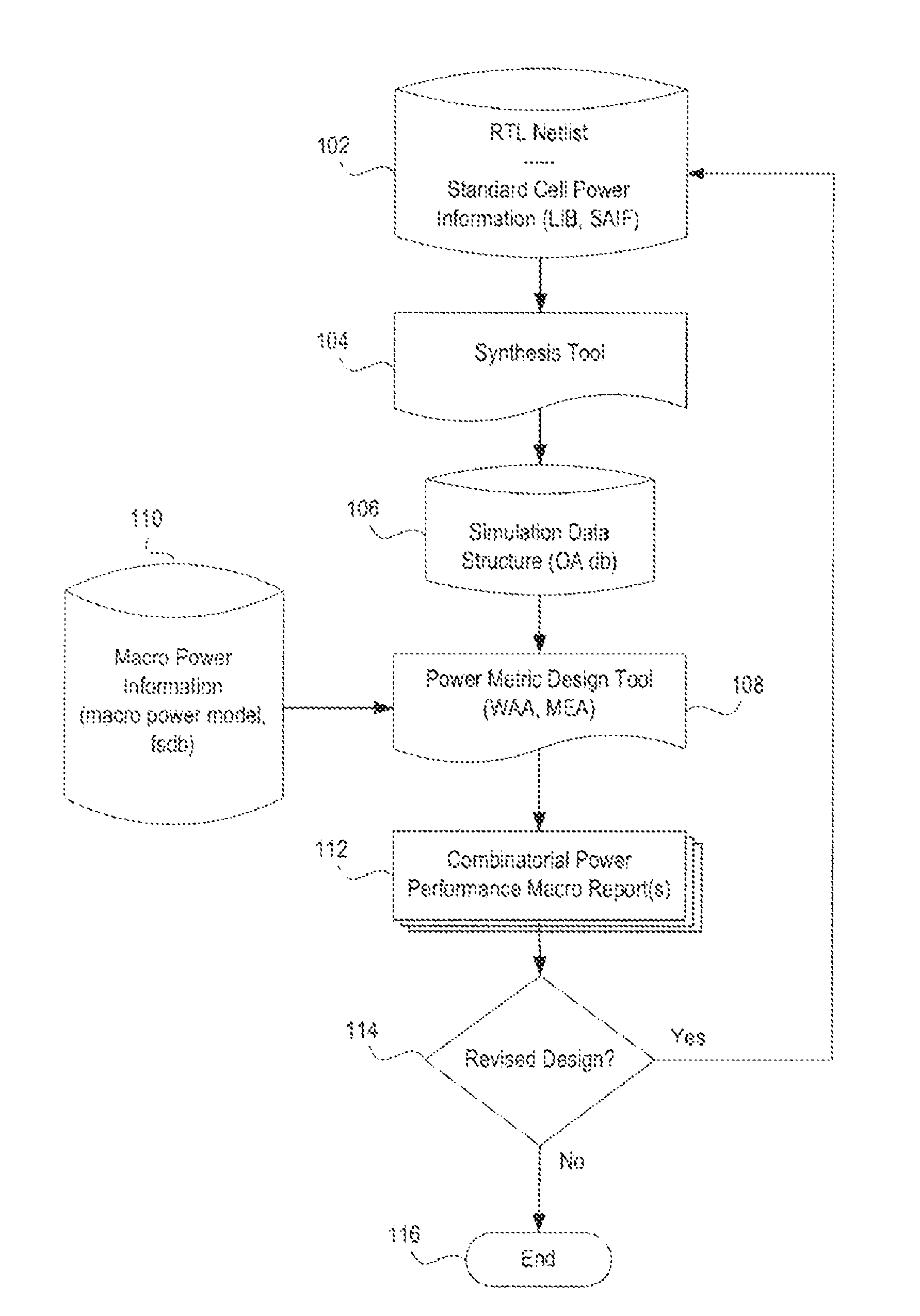
[0006]Broadly speaking, the present invention provides a system, method and apparatus for designing an electronic device to have reduced power consumption by efficiently tracking power efficiency for one or more circuit blocks or modules using a combinatorial power performance metric that is defined to allow identification of critical enables to flip-flops and arrays in order to improve switching factor, and reduce capacitance loads on active nets. In operation, a design tool receives and evaluates an RTL design using atomic combinatorial power performance metrics to identify gating enable conditions which optimize power performance for the circuit by maximizing a weighted activity metric that is defined in terms of capacitance, switching activity and power effort. By combining switching activity, effective switching capacitance, and power effort into a single atomic metric, power consumption may be more accurately and efficiently estimated to track power efficiency improvements and...
PUM
 Abstract
Description
Claims
Application Information