Method of processing silicon substrate and method of manufacturing substrate for liquid discharge head

a technology of silicon substrate and manufacturing substrate, which is applied in the direction of recording equipment, recording information storage, instruments, etc., can solve the problems of reducing the width size of the liquid discharge head, reducing the manufacturing efficiency, and requiring a large amount of laser processing of the trenches, so as to achieve the effect of small width

Inactive Publication Date: 2012-10-16
CANON KK
View PDF13 Cites 4 Cited by
  • Summary
  • Abstract
  • Description
  • Claims
  • Application Information

AI Technical Summary

Benefits of technology

[0010]Thus, an object of the present invention is to provide a method of processing a silicon substrate that can form a penetration port with a small width in the silicon substrate so as to form the penetration port effectively and a method of manufacturing a substrate for a liquid discharge head.
[0014]According to the present invention, the penetration port can be formed while suppressing the expansion of the transverse width (in a plane direction), an effective method of processing the silicon substrate and a method of manufacturing the substrate for the liquid discharge head can be provided.

Problems solved by technology

In this method, a large amount of inscription of a trench with a laser processing is required.
However, there is a problem in that time required for the laser processing is extended along with an increase in amount of inscription by the laser processing, which reduces the manufacturing efficiency.
However, even in this method, the section of the ink supply port is also formed in the expanded shape, and thus there is a limitation in the reduction of the width size of the liquid discharge head.
However, in this process, the etching time for forming the ink supply port is long and the passage width of the opposite surface of the silicon substrate is extended in the transverse direction, which makes it difficult to reduce the ink jet head.
However, if the etching rates of the respective plane orientations of the anisotropic etching are not controlled, the width of the ink supply port is widened due to the time of the anisotropic etching, and thus, there is a problem in that the elimination amount of the silicon is large, which lowers the production efficiency.

Method used


Image

  • Method of processing silicon substrate and method of manufacturing substrate for liquid discharge head
  • Method of processing silicon substrate and method of manufacturing substrate for liquid discharge head
  • Method of processing silicon substrate and method of manufacturing substrate for liquid discharge head

Examples


first example

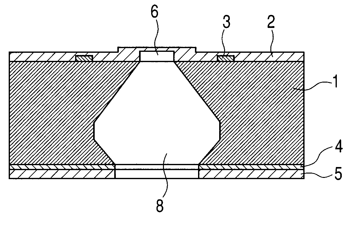
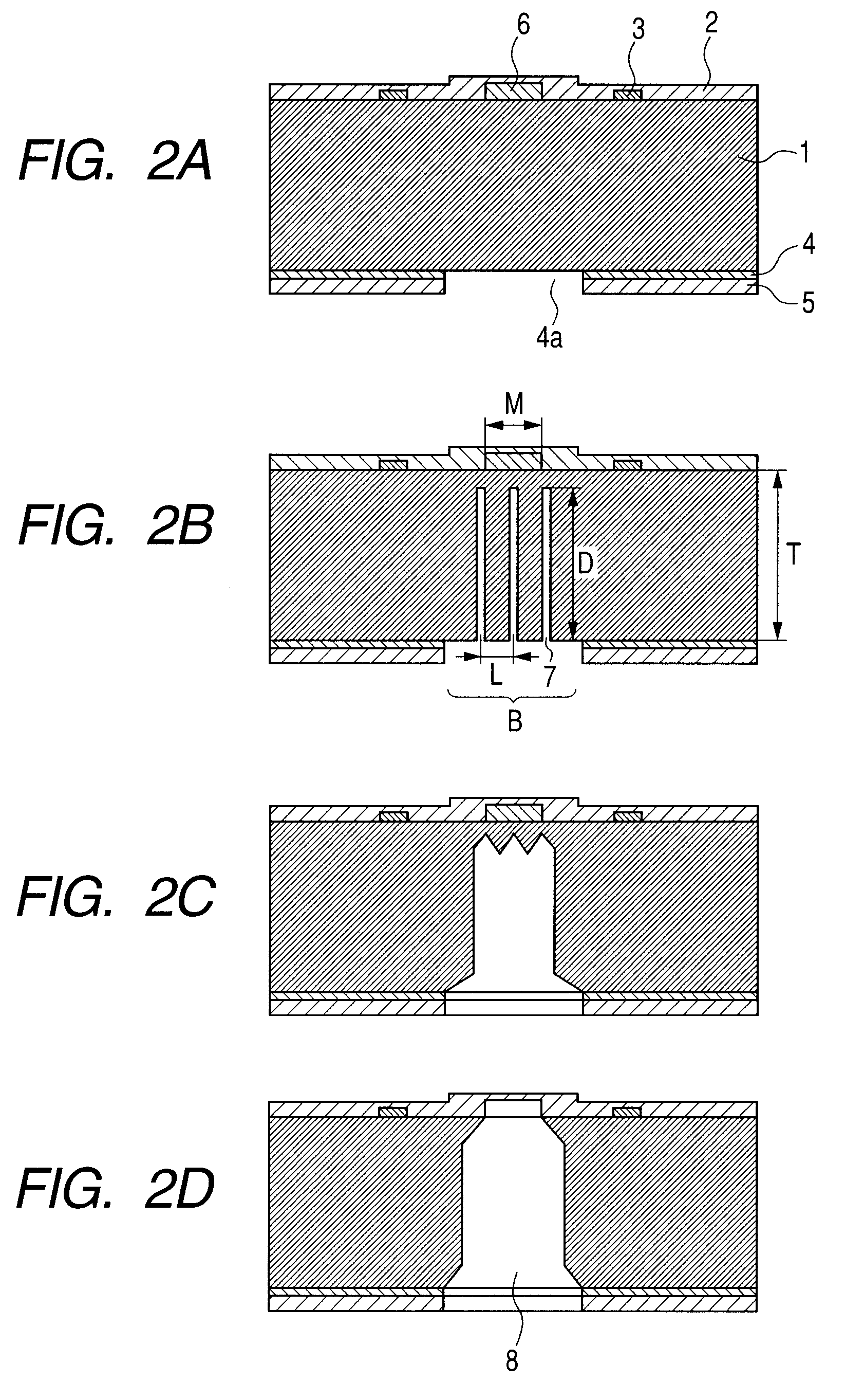
[0051]As illustrated in FIG. 2A, polyether amide resin was overlaid on the SiO2 layer 4 of the opposite surface of the silicon substrate 1 to form the etching mask layer 5 with an opening portion. The silicon substrate with thickness of 725 μm was used. The SiO2 layer 4 was removed from the opening portion.

[0052]Next, as illustrated in FIG. 2B, the leading holes 7 were formed by the laser processing in the opening portion of the etching mask layer 5. By setting the depth of the laser processing to be 650 μm and the pitch distance to be 60 μm in the longitudinal and transverse directions, three rows of leading holes were formed in the transverse direction.

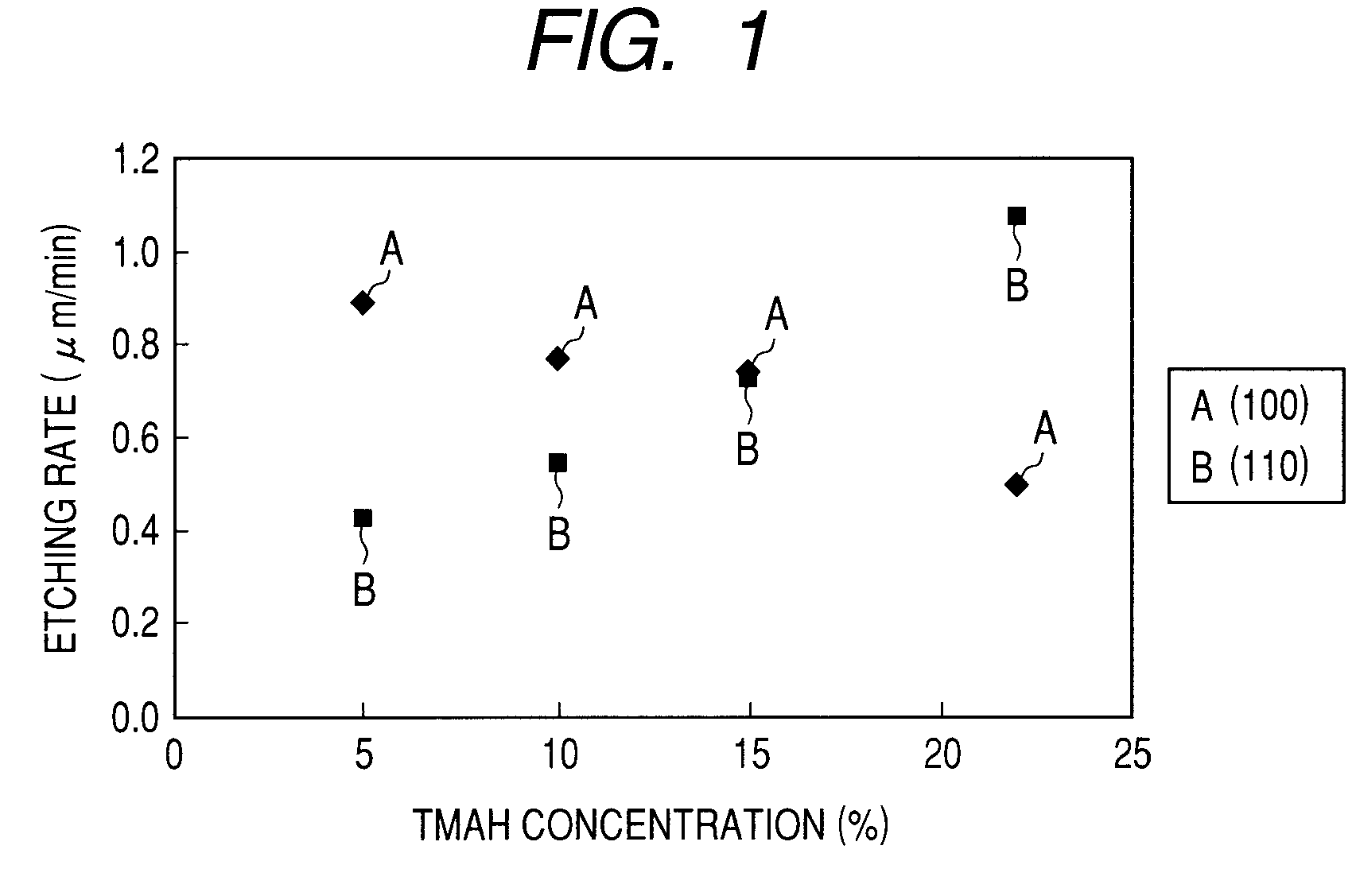
[0053]Next, as illustrated in FIG. 2C, the crystalline anisotropic etching was executed from the opposite surface of the silicon substrate using TMAH 10 wt %.

[0054]In the case of TMAH 10 wt %, the etching rate of the (100) surface is 1.124 μm / min. On the other hand, the etching rate of the (110) surface is 0.789 μm / min. Thus, the et...


PUM

PropertyMeasurementUnit
thicknessaaaaaaaaaa
THG: wavelengthaaaaaaaaaa
diametersaaaaaaaaaa

Abstract

A method of processing a substrate includes the steps of providing a silicon substrate that has an etching mask layer with an opening portion at a first surface thereof and has plane orientation of {100} with the surface of the silicon being exposed from the opening portion; preparing a recessed portion that faces from the first surface to a second surface, opposite to the first surface, in the opening portion of the silicon substrate; and forming a penetration port that passes through the first surface and the second surface of the silicon substrate by executing crystalline anisotropic etching in the silicon substrate using an etching liquid in which an etching rate for etching a (100) surface of silicon is higher than an etching rate for etching a (110) surface of silicon, from the recessed portion of the silicon substrate toward the second surface.

Description

BACKGROUND OF THE INVENTION[0001]1. Field of the Invention[0002]The present invention relates to a method of processing a silicon substrate so as to form a penetration port in the silicon substrate and a method of manufacturing a substrate for a liquid discharge head that discharges a liquid such as an ink to a material to be recorded such as a recording paper.[0003]2. Description of the Related Art[0004]A method of manufacturing an ink jet recording head which is a typical example of the liquid discharge head is described in the following patent documents.[0005]Japanese Patent Application Laid-open No. 2004-148824 discloses a method of manufacturing an ink jet recording head by etching silicon after having been subjected to a trench processing by laser. In this method, a large amount of inscription of a trench with a laser processing is required. However, there is a problem in that time required for the laser processing is extended along with an increase in amount of inscription by...

Claims


Application Information

Patent Timeline
Patent Type & Authority Patents(United States)
IPC IPC(8): H01B13/00
CPCB41J2/1603B41J2/1631B41J2/1629
Inventor KISHIMOTO, KEISUKEYONEMOTO, TAICHI
Owner CANON KK
Why Eureka
Try Eureka