Gallium and nitrogen containing triangular or diamond-shaped configuration for optical devices

a technology of gallium and nitrogen and optical devices, applied in semiconductor devices, semiconductor/solid-state device testing/measurement, electrical equipment, etc., can solve the problems of high intensity, conventional edison light bulbs are routinely failed, and the conventional edison light bulb fails to achieve high intensity, etc., to achieve easy cleavage, improve light extraction, and yield. high

Active Publication Date: 2012-10-23
KORRUS INC
View PDF45 Cites 36 Cited by
  • Summary
  • Abstract
  • Description
  • Claims
  • Application Information

AI Technical Summary

Benefits of technology

[0017]In a specific embodiment, the invention provides for a method for singulation of thick c-plane GaN wafers into triangle-shaped LED chips defined by three equivalent m-plane oriented sidewalls. In one or more embodiments, the m-plane is a natural break plane, which easily cleaves, in the case of c-plane GaN wafers, and therefore, a singulation process involving breaking exclusively or predominately along a set of m-plane orientations will have a higher yield than a process involving breaking along both m-plane orientations and a-plane orientations. In another specific embodiment, the present invention provides for a method for singulation of c-plane GaN wafers into triangle-shaped LED chips defined by three equivalent m-plane oriented sidewalls. In one or more embodiments, break along the a-plane yields a characteristic surface texture which results in improved light extraction.
[0018]The invention provides triangle-shaped chips characterized by improved light extraction when compared to conventional square- or rectangle-shaped chips, due to an increase in the per-pass probability of escape of in-plane emission arising from a decrease in the probability of total internal reflection at the sidewalls. Additionally, triangle-shaped chips provide fewer trapped trajectories of light than square or rectangle chips, so that the chip light extraction efficiency can be increased.

Problems solved by technology

Unfortunately, drawbacks exist with the conventional Edison light bulb.
Additionally, the conventional light bulb routinely fails often due to thermal expansion and contraction of the filament element.
Unfortunately, achieving high intensity, high-efficiency GaN-based green LEDs has been particularly problematic.
Additionally, GaN based LEDs have been costly and difficult to produce on a wide-scale in an efficient manner.

Method used


Image

  • Gallium and nitrogen containing triangular or diamond-shaped configuration for optical devices
  • Gallium and nitrogen containing triangular or diamond-shaped configuration for optical devices
  • Gallium and nitrogen containing triangular or diamond-shaped configuration for optical devices

Examples


Embodiment Construction

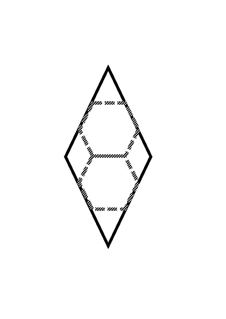
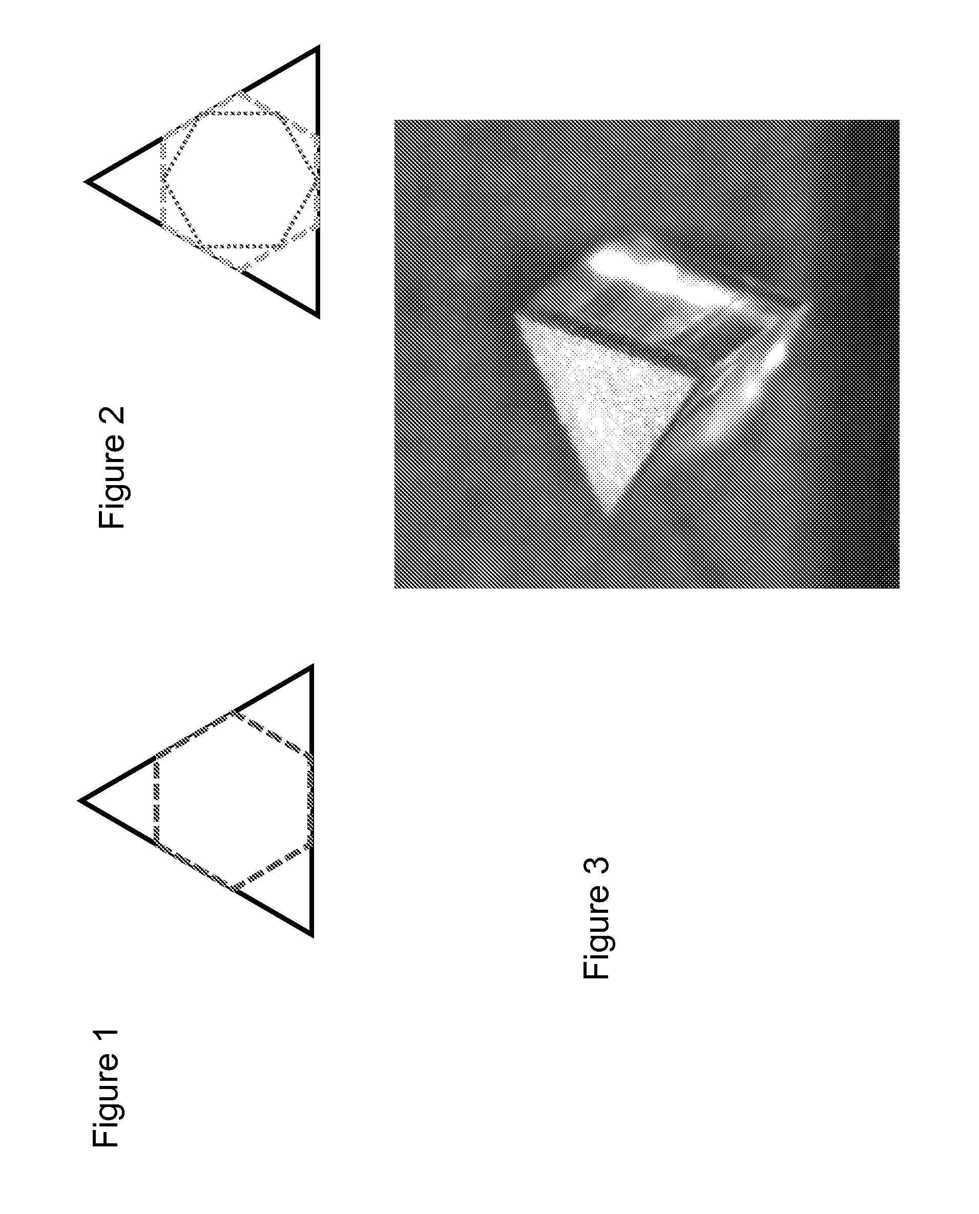
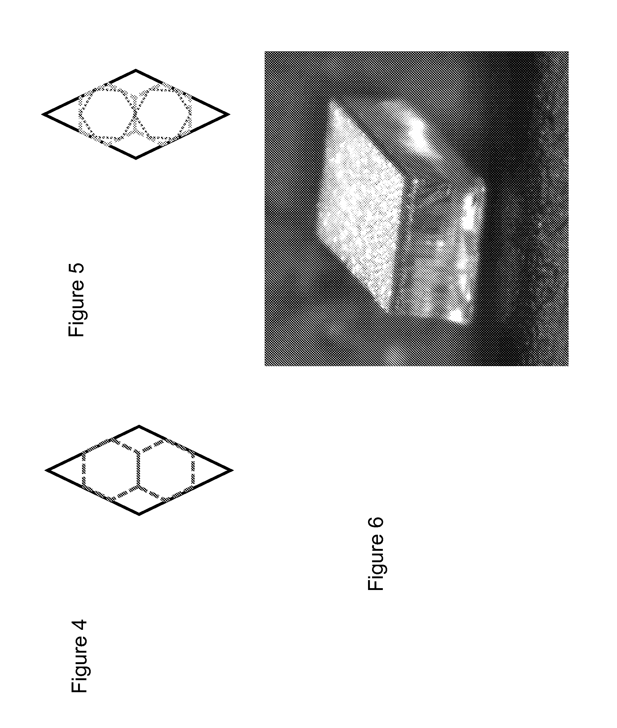
[0026]FIGS. 1 through 3 are simplified diagrams illustrating a method for forming a triangular shaped gallium and nitrogen containing material according to an embodiment of the present invention. As shown in FIG. 1, the invention provides a gallium and nitrogen containing substrate member. The member includes a gallium and nitrogen containing thickness of material configured in a triangular shape consisting of no more than five surface regions. Preferably, the five surface regions comprises a three surface regions configured from respective first equivalent planes and the five surface regions excluding the three surface regions comprises two surface regions configured from second equivalent planes. As shown is a top-view of a triangular shaped chip showing orientation of three edges relative to GaN m-planes according to a specific embodiment (see dashed or red lines).

[0027]In a specific embodiment, the gallium and nitrogen containing substrate is triangular shaped. The triangular sh...


PUM


Abstract

A gallium and nitrogen containing optical device has a base region and no more than three major planar side regions configured in a triangular arrangement provided from the base region.

Description

CROSS REFERENCE TO RELATED APPLICATION[0001]This application claims priority to U.S. Provisional Application No. 61 / 356,473, filed Jun. 18, 2010, which is incorporated herein by reference for all purposes.BACKGROUND OF THE INVENTION[0002]This invention relates generally to lighting techniques. More specifically, embodiments of the invention include techniques for manufacturing optical devices, such as light emitting diodes (LEDs) using a separation process of thick gallium and nitrogen containing substrate members, such as GaN configured in polar crystalline orientations. In some embodiments, the gallium and nitrogen containing substrate is configured in a triangular shape or a diamond shape. The invention can be applied to applications such as white lighting, multi-colored lighting, general illumination, decorative lighting, automotive and aircraft lamps, street lights, lighting for plant growth, indicator lights, lighting for flat panel displays, and other optoelectronic devices.[...

Claims


Application Information

Patent Timeline
Patent Type & Authority Patents(United States)
IPC IPC(8): H01L21/66
CPCH01L33/0095H01L33/20
Inventor SHARMA, RAJATFELKER, ANDREW
Owner KORRUS INC
Why Eureka
Try Eureka