Lateral extended drain metal oxide semiconductor field effect transistor (LEDMOSFET) with tapered dielectric plates

a technology of field effect transistor and metal oxide semiconductor, which is applied in the field of extended drain, metal oxide semiconductor, field effect transistor (ledmosfet), can solve the problems of corresponding decrease in switching speed and limit of device size scaling, and achieve high drain-to-body breakdown voltage, efficient depletion, and increase width

Inactive Publication Date: 2012-10-30
GLOBALFOUNDRIES INC
View PDF28 Cites 5 Cited by
  • Summary
  • Abstract
  • Description
  • Claims
  • Application Information

AI Technical Summary

Benefits of technology

[0007]In view of the foregoing, disclosed herein are embodiments of a lateral, extended drain, metal oxide semiconductor, field effect transistor (LEDMOSFET) having a relatively high drain-to-body breakdown voltage (Vb). The LEDMOSFET embodiments have gate structure extensions that are positioned adjacent to opposing sides of the drain drift region and function as conductive field plates. In one embodiment, these extensions extend vertically through the isolation region that surrounds the LEDMOSFET. In another embodiment, the extensions sit atop the isolation region. In either case, each extension has a sidewall that is angled relative to the drain drift region such that the portion of the isolation region between the extension and the drain drift region (i.e., the portion of the isolation region that functions as a dielectric field plate) has a continuously increasing width along the length of the drain drift region from the channel region to the drain region. This dielectric field plate, which is tapered from the drain region to the channel region, creates a strong essentially uniform horizontal electric field profile within the drain drift. Such an electric field profile limits the transverse field to the nwell / pwell junction, limits the ionization rate to safe, low values and allows the drain drift region to be efficiently depleted so that a relatively high specific drain-to-body breakdown voltage is achieved.
[0017]It should be noted that in each of the above-described method embodiment, prior to gate structure formation, the dimensions of the portion of the isolation region between each extension and the drain drift region and, thereby, the dimensions of each extension can be defined based on various specifications set forth in the design for the drain drift region (e.g., based on a specified width, a specified length, a specified height, and a specified doping profile for the drain drift region) so as to create a strong essentially uniform horizontal electric field profile within the drain drift region of the field effect transistor. Such an electric field profile limits the transverse field to the nwell / pwell junction, limits the ionization rate to a safe, low value and allows the drain drift region to be efficiently depleted. Thus, a relatively high specific drain-to-body breakdown voltage (Vb) can be achieved.

Problems solved by technology

However, device size scaling has its limits because short channel lengths can also lead to a number of undesirable “short-channel effects”.
Unfortunately, halos with a relatively high dopant concentration can also cause a corresponding decrease in switching speed.

Method used


Image

  • Lateral extended drain metal oxide semiconductor field effect transistor (LEDMOSFET) with tapered dielectric plates
  • Lateral extended drain metal oxide semiconductor field effect transistor (LEDMOSFET) with tapered dielectric plates
  • Lateral extended drain metal oxide semiconductor field effect transistor (LEDMOSFET) with tapered dielectric plates

Examples


Embodiment Construction

[0040]The embodiments of the invention and the various features and advantageous details thereof are explained more fully with reference to the non-limiting embodiments that are illustrated in the accompanying drawings and detailed in the following description.

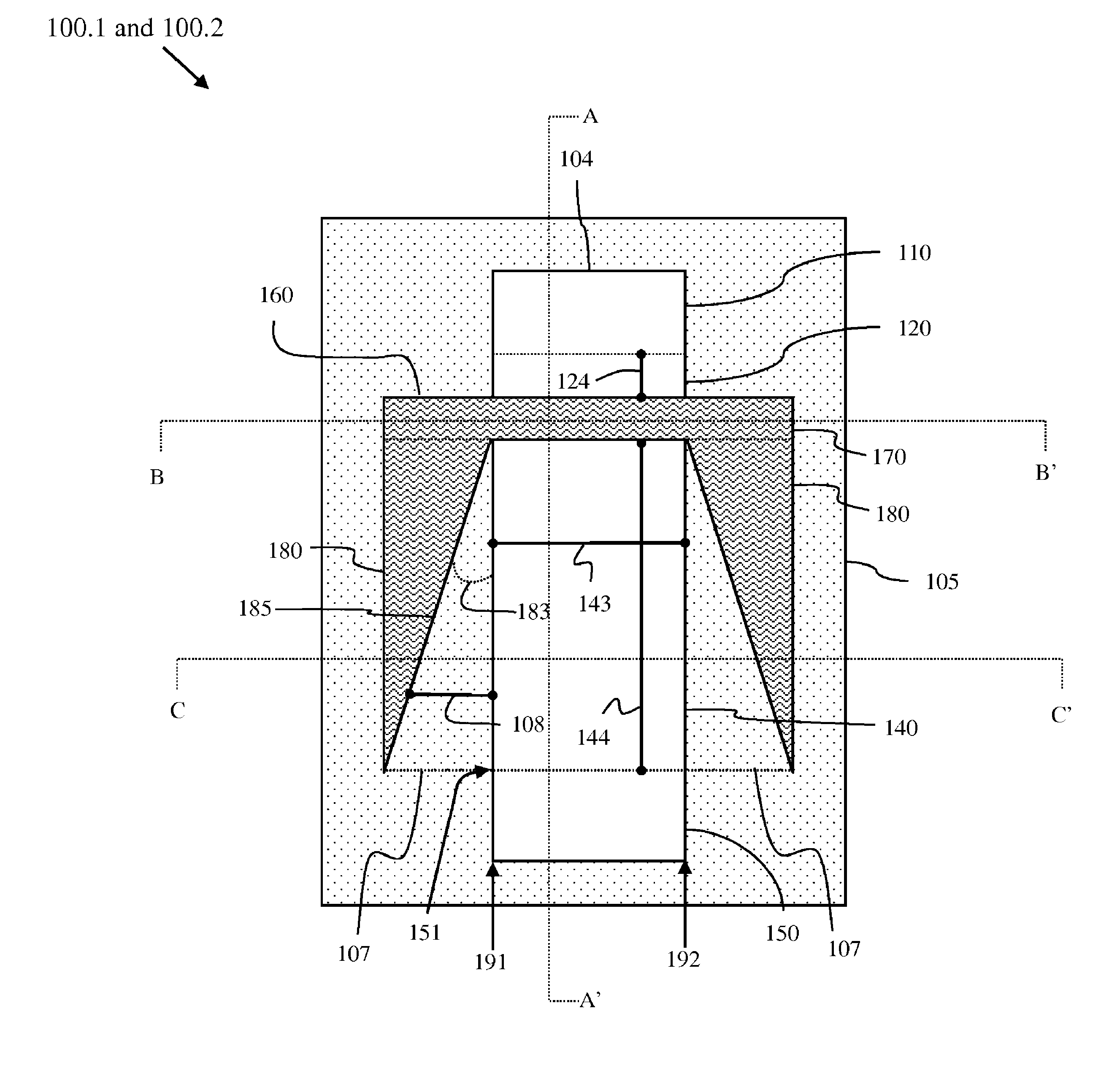
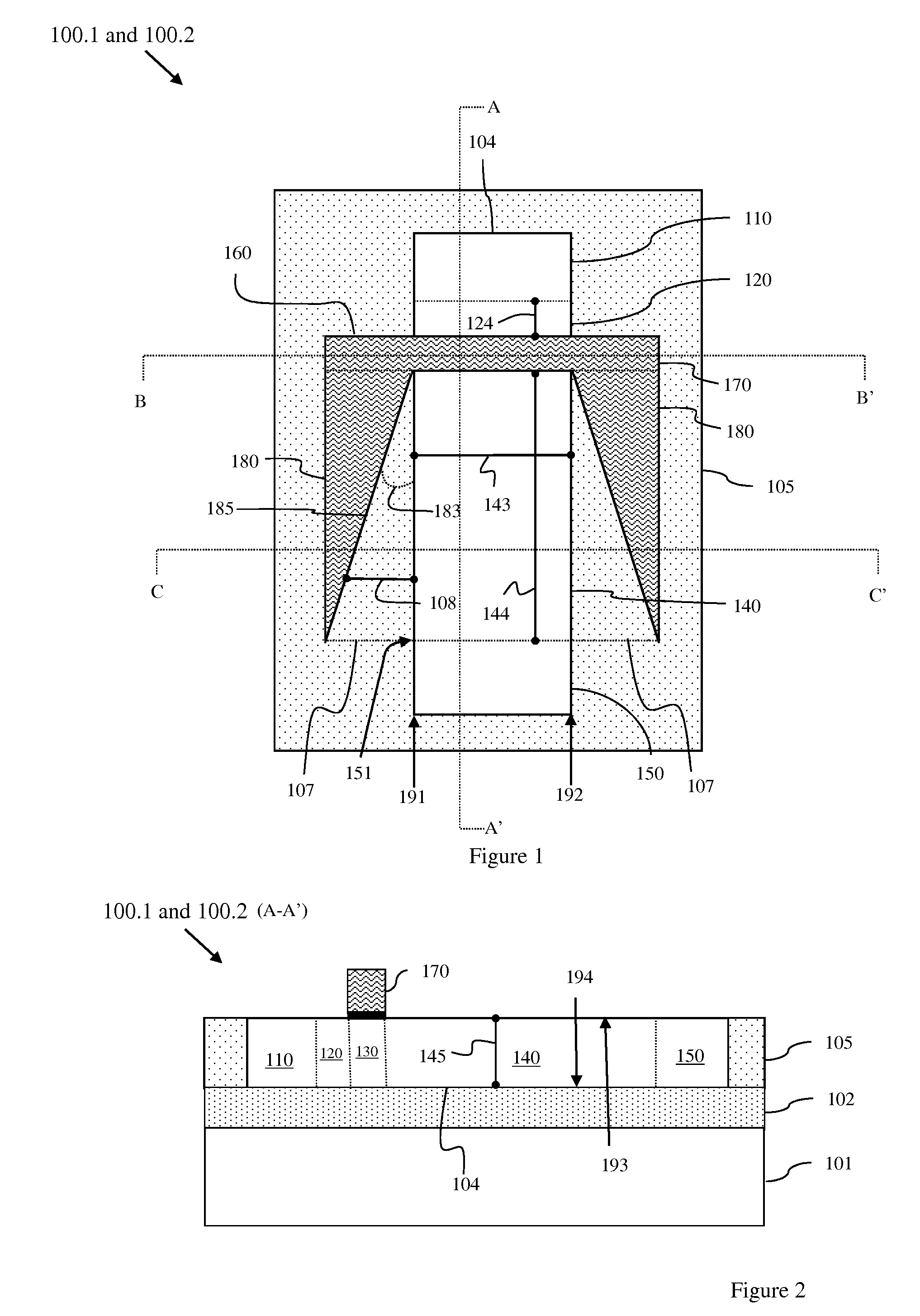
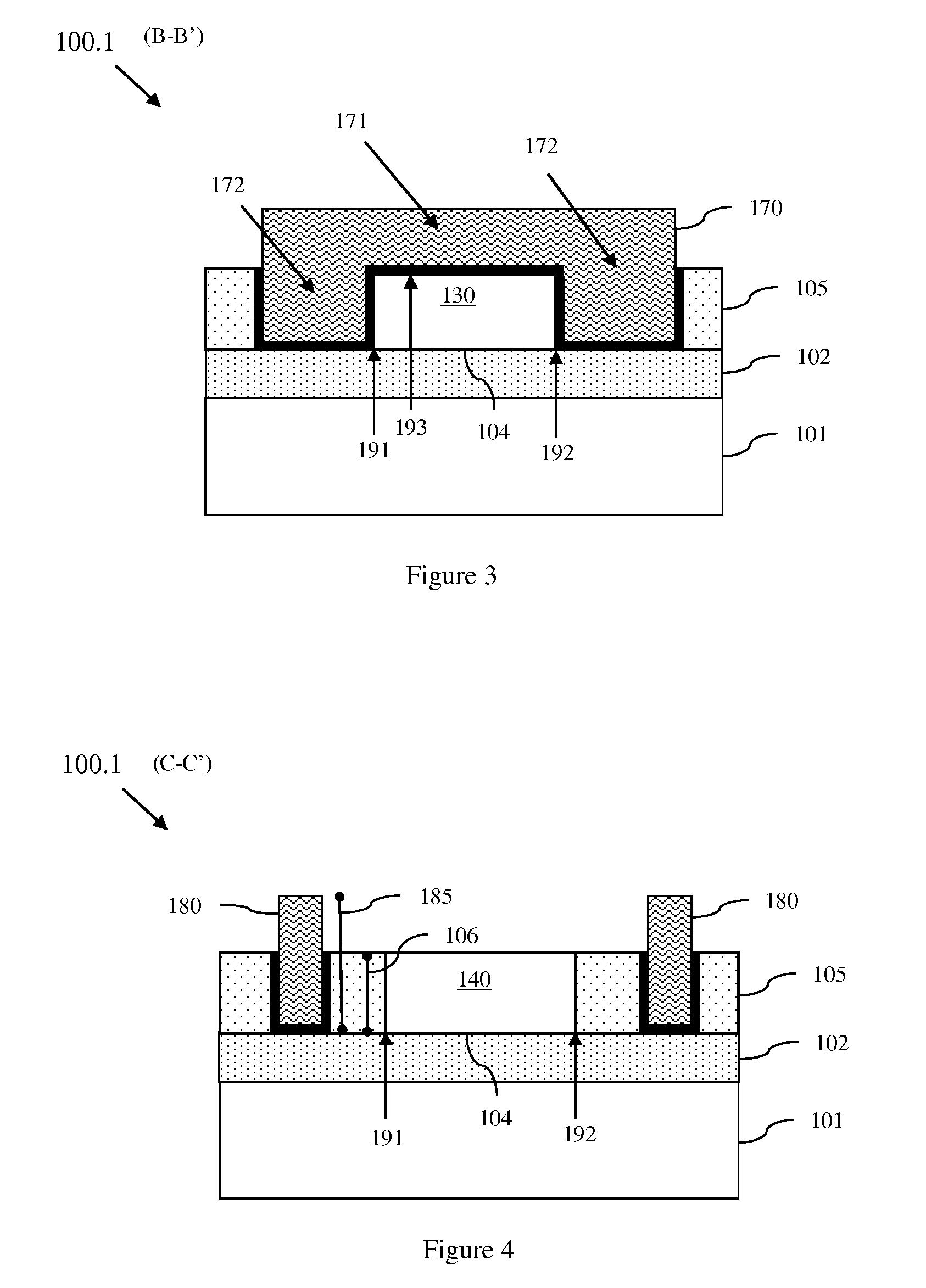
[0041]As mentioned above, field effect transistor structures have been developed that balance the need to reduce the short channel effects exhibited by a scaled device with the need for a faster switching speed. For example, one such field effect transistor structure is a lateral, extended drain, metal oxide semiconductor, field effect transistor (LEDMOSFET) that is asymmetric with respect to the source / drain drift region configuration (e.g., the drain drift region can be longer than the source drift region, if any, and can have a lower dopant concentration). Optionally, an LEDMOSFET can also be asymmetric with respect to the halo configuration (e.g., a source-side halo only). Such an LEDMOSFET provides decreased source resist...


PUM


Abstract

A lateral, extended drain, metal oxide semiconductor, field effect transistor (LEDMOSFET) with a high drain-to-body breakdown voltage (Vb) incorporates gate structure extensions on opposing sides of a drain drift region. The extensions are tapered such that a distance between each extension and the drift region increases linearly from one end adjacent to the channel region to another end adjacent to the drain region. In one embodiment, these extensions can extend vertically through the isolation region that surrounds the LEDMOSFET. In another embodiment, the extensions can sit atop the isolation region. In either case, the extensions create a strong essentially uniform horizontal electric field profile within the drain drift. Also disclosed are a method for forming the LEDMOSFET with a specific Vb by defining the dimensions of the extensions and a program storage device for designing the LEDMOSFET to have a specific Vb.

Description

BACKGROUND[0001]1. Field of the Invention[0002]The present invention relates to a lateral, extended drain, metal oxide semiconductor, field effect transistors (LEDMOSFETs) and, more specifically, to embodiments of a LEDMOSFET having tapered dielectric plates to achieve a relatively high drain-to-body breakdown voltage, a method of forming the LEDMOSFET and a program storage device for designing the LEDMOSFET.[0003]2. Description of the Related Art[0004]Generally, integrated circuit structures are designed with the following goals in mind: (1) decreasing device size; (2) increasing device performance (e.g., by increasing switching speed) and (3) decreasing power consumption. Device size scaling can lead to a corresponding decrease in device channel lengths and, thereby a corresponding increase in switching speed. However, device size scaling has its limits because short channel lengths can also lead to a number of undesirable “short-channel effects”. These short-channel effects inclu...

Claims


Application Information

Patent Timeline
Patent Type & Authority Patents(United States)
IPC IPC(8): H01L21/336
CPCH01L29/402H01L29/407H01L29/4238H01L29/66681H01L29/66704H01L29/66795H01L29/7824H01L29/7825H01L29/785G06F17/5063G06F30/36
Inventor ABOU-KHALIL, MICHEL J.BOTULA, ALAN B.JOSEPH, ALVIN J.LETAVIC, THEODORE J.SLINKMAN, JAMES A.
Owner GLOBALFOUNDRIES INC
Why Eureka
Try Eureka