Power switch design method and program

a technology of power switch and design method, applied in the field of power switch design method and program, can solve the problems of complex ic design, difficult to accurately meet performance requirements, and add area overhead, and achieve the effect of high capacitive driving capacity

Inactive Publication Date: 2012-10-30
NXP BV
View PDF13 Cites 9 Cited by
  • Summary
  • Abstract
  • Description
  • Claims
  • Application Information

AI Technical Summary

Benefits of technology

[0010]By providing a stack of the drivers and a small power switch in combination with optimizing the layout of the power switches instead of using standard switches from a predefined library, a highly area-efficient power supply block is obtained. Moreover, the optimization of the power switch layout allows for an accurate compliance of the power switch block with its performance requirements.
[0011]Preferably, the step of optimizing the first power switch layout comprises optimizing at least one of the gate length and the number of fingers of the first power switch such that a difference between the optimized width / length ratio of the first power switch and the predefined width / length ratio is minimized.
[0016]In a further embodiment, the method further comprises providing a library of components in the predefined integrated circuit technology, said library including a plurality of drivers having different capacitive driving capabilities; and selecting the pair of drivers from said library based on the respective loads of the first power switch and the second power switch. This way, it is ensured that the area overhead is minimized by ensuring that the smallest possible driver is selected.
[0017]Advantageously, the further embodiment further comprises finding, in said library, the driver having the highest capacitive driving capacity; comparing said driving capacity with the load of the corresponding power switch; and, in case the load exceeds said driving capacity, adding a further segment to the power switch block; and dividing said load over the segment and the further segment. This has the advantage that it can be determined early on in the design process how many segments are required in the power switch block, thus enabling an area-efficient design of each segment. Typically, because the overall load is balanced over the segments, these segments are substantially identical to each other.
[0018]In another embodiment, the predefined width / length ratios are calculated from the desired respective resistances of said power switches. This ensures a good match between the desired performance properties of the power switch block and its actual performance properties following the layout optimization of the respective power switches.
[0019]According to another aspect of the present invention, there is provided a computer program product comprising computer code means arranged to, when executed on a computer, implement the steps of the method according to the present invention. Such computer code means, which may comprise algorithms and instructions to implement the method of the present invention, has the advantage that an IC design comprising area-optimized power switch blocks can be automatically provided. Such a program product may be stored on a computer-readable data carrier such as a DVD, a CD-ROM, a memory stick, an internet-accessible hard disk and so on.

Problems solved by technology

This not only adds area overhead but also complexity to the IC design because a substantial number of interconnections has to be provided for.
In addition, the use of standard transistors may make it difficult to accurately meet the performance requirements.

Method used


Image

  • Power switch design method and program
  • Power switch design method and program
  • Power switch design method and program

Examples


Embodiment Construction

[0031]It should be understood that the Figures are merely schematic and are not drawn to scale. It should also be understood that the same reference numerals are used throughout the Figures to indicate the same or similar parts.

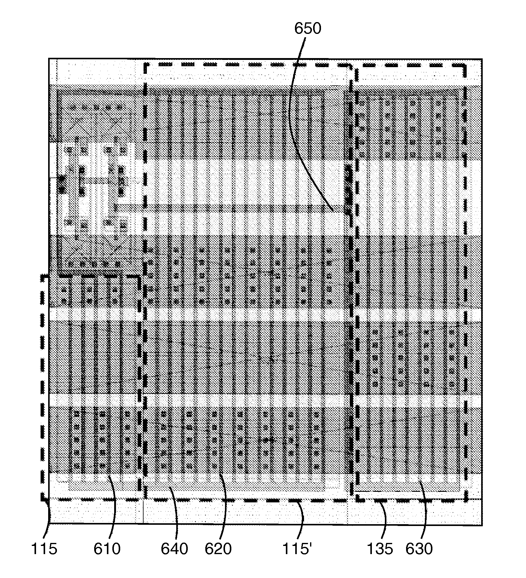
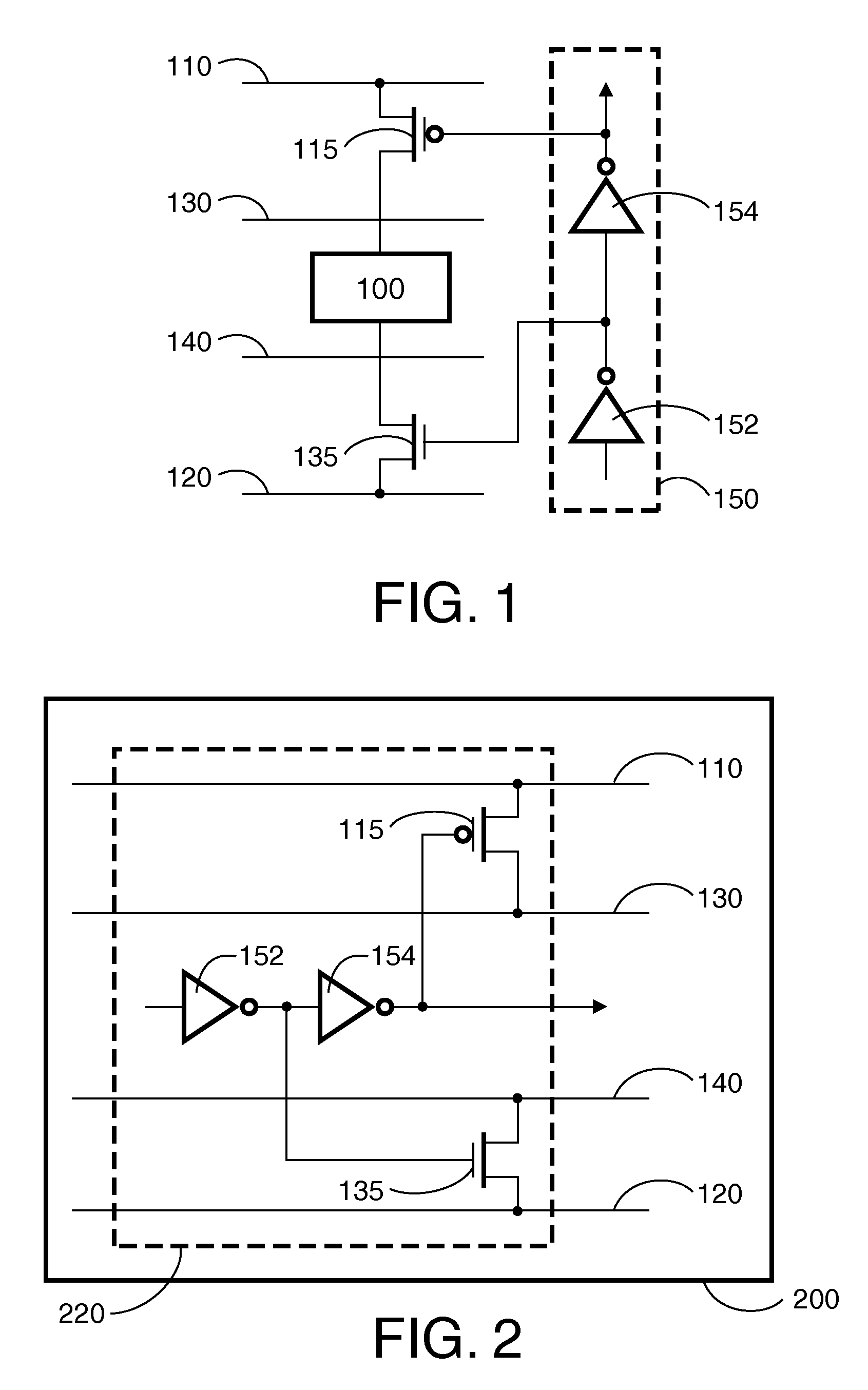
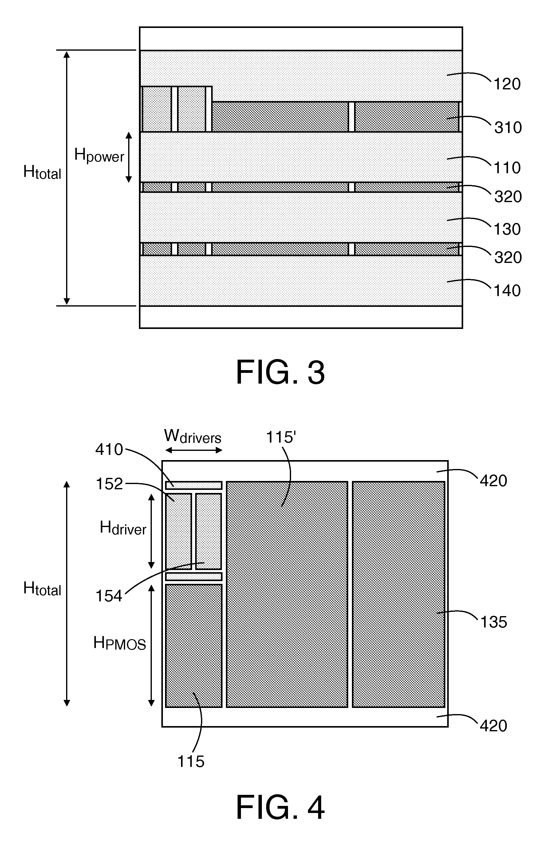
[0032]In accordance with the method of the present invention, the dimension of the power switch block 200 is designed in such a way that the total area covered by the power switch block 200 is minimized. The method of the present invention is based on the realization that for a given IC technology, although the various components of the power switch block 200 may have dimensions that are more or less fixed within the given IC technology, the layout of some components, such as the first power switch 115 and the second power switch 135 may be optimized within the dimensions constraints to optimize the performance of such a component within the power switch block 200. In other words, some components are designed on-the-fly instead of taken from a standard librar...


PUM


Abstract

A method of designing a power switch block (200) for an integrated circuit layout in a predefined integrated circuit technology is disclosed. The power switch block (200) includes a segment (710) comprising a plurality of spaced parallel conductors (110, 120, 130, 140) each having a predefined height in said technology, a stack of a first power switch (115) of a first conductivity type and a pair of drivers (152; 154) for respectively driving the first power switch (115) and a second power switch (135), said drivers having predefined dimensions in said technology, and the second switch (135) of a second conductivity type. The method comprises providing respective predefined width / length ratios for said power switches (115; 135); determining a total height of the segment (710) from the sum of the predefined heights of the individual conductors (110; 120; 130; 140) and respective spacings (310; 320) between said individual conductors, determining the height of the first transistor (115) from the difference between the total height and the predefined driver height; determining the width of the first transistor (115) from the combined predefined widths of the pair of drivers (152; 154); optimizing the first power switch layout within its determined height and width based on its predefined width / length ratio; and optimizing the second power switch layout based on its predefined width / height ratio.

Description

FIELD OF THE INVENTION[0001]The present invention relates to a method of designing a power switch block for an integrated circuit layout in a predefined integrated circuit technology.[0002]The present invention further related to a computer program product implementing such a method.BACKGROUND OF THE INVENTION[0003]Nowadays, many integrated circuits (ICs) are designed to perform a wide variety of computational tasks. To this end, such an IC may comprise a plurality of different circuit portions, e.g. cores, each designed to perform one of said computational tasks. An example of such a multi-tasking IC design is the system-on-chip concept. Usually, such ICs perform only a subset of the computational tasks at the same time, which means that the other circuit portions do not perform any tasks. To avoid unnecessary power consumption by such idle circuit portions, these circuit portions are temporarily disconnected from the power supply until their functionality is required again.[0004]T...

Claims


Application Information

Patent Timeline
Patent Type & Authority Patents(United States)
IPC IPC(8): G06F17/50
CPCG06F17/5072G06F30/392
Inventor PINEDA DE GYVEZ, JOSE DE JESUSMEIJER, RINZE IDA MECHTILDIS PETERGROOT, CAS
Owner NXP BV
Why Eureka
Try Eureka