Power semiconductor device

a technology of semiconductor devices and semiconductors, applied in the field of power electronics, can solve problems such as limiting trench est performance at a level comparabl

Active Publication Date: 2012-11-06
HITACHI ENERGY SWITZERLAND AG
View PDF1 Cites 10 Cited by
  • Summary
  • Abstract
  • Description
  • Claims
  • Application Information

AI Technical Summary

Benefits of technology

[0037]The horizontally stacked super junction layers in the form of stacked enhancement layer(s) and well layer(s) in the MOS cell circumvent the peak electric field near the junction. By the repetitive introduction of an additional enhancement layer and additional well, the doping concentration for each layer can be enhanced so that the ohmic conductivity is enhanced and thereby better carrier spreading properties surpassing the possibilities of the conventional n-type enhancement layer below the trench IGBT p-base layer can be achieved. Thus, the on-state losses are reduced.
[0040]According to an exemplary embodiment, the total conductivity of the MOS cells is a mix of ohmic and bipolar conduction with a very high share contributed by the ohmic part; this allows fast dynamics due to the low amount of emitter-side bipolar carrier modulation.
[0041]The feature of the additional enhancement layer(s) and addition well layer(s) can be combined with a super-junction structure, in which the additional well layer includes an additional well layer bottom, which is arranged closer to the collector side than the gate bottom. By having an additional well layer bottom close to the gate bottom or even closer to the collector side than the gate bottom, high peaking electric fields at the trench corner are reduced or even avoided, thereby further reducing switching losses of the device.
[0042]The layout of the stacked enhancement and well layers results in a coupling of the depletion at the top PN junction with the n-drift layer (vertical super junction base) depletion; the device can thus be designed to provide current saturation and short circuit capability.

Problems solved by technology

However, this limits the trench EST performance at a level comparable to conventional trench insulated gate bipolar transistors (IGBTs) employing n-type enhancement layers.

Method used


Image

  • Power semiconductor device
  • Power semiconductor device
  • Power semiconductor device

Examples


Embodiment Construction

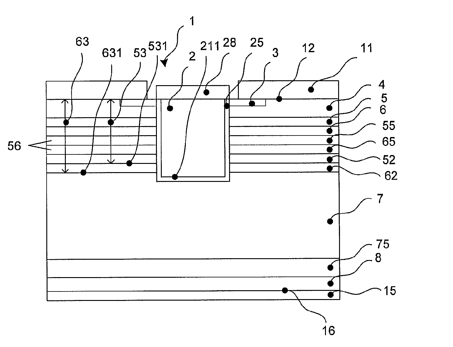
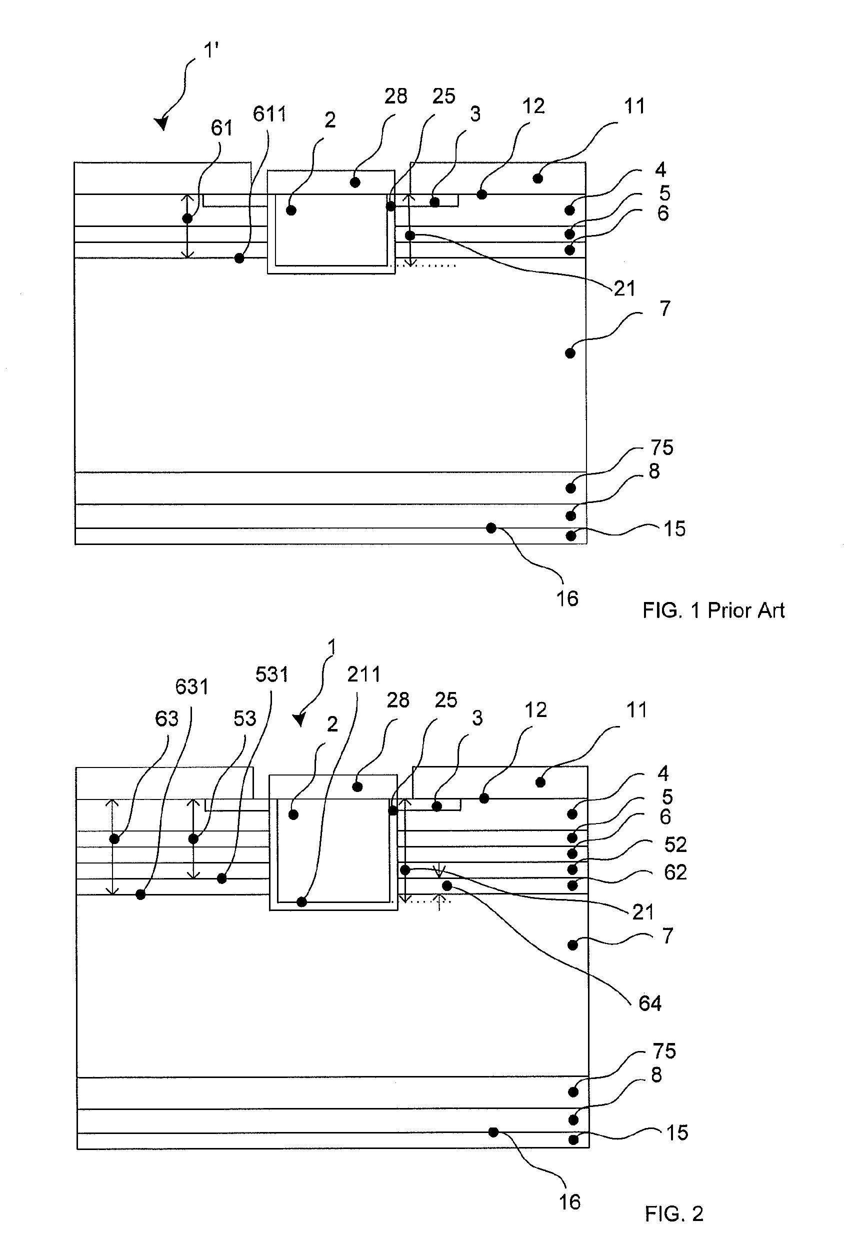
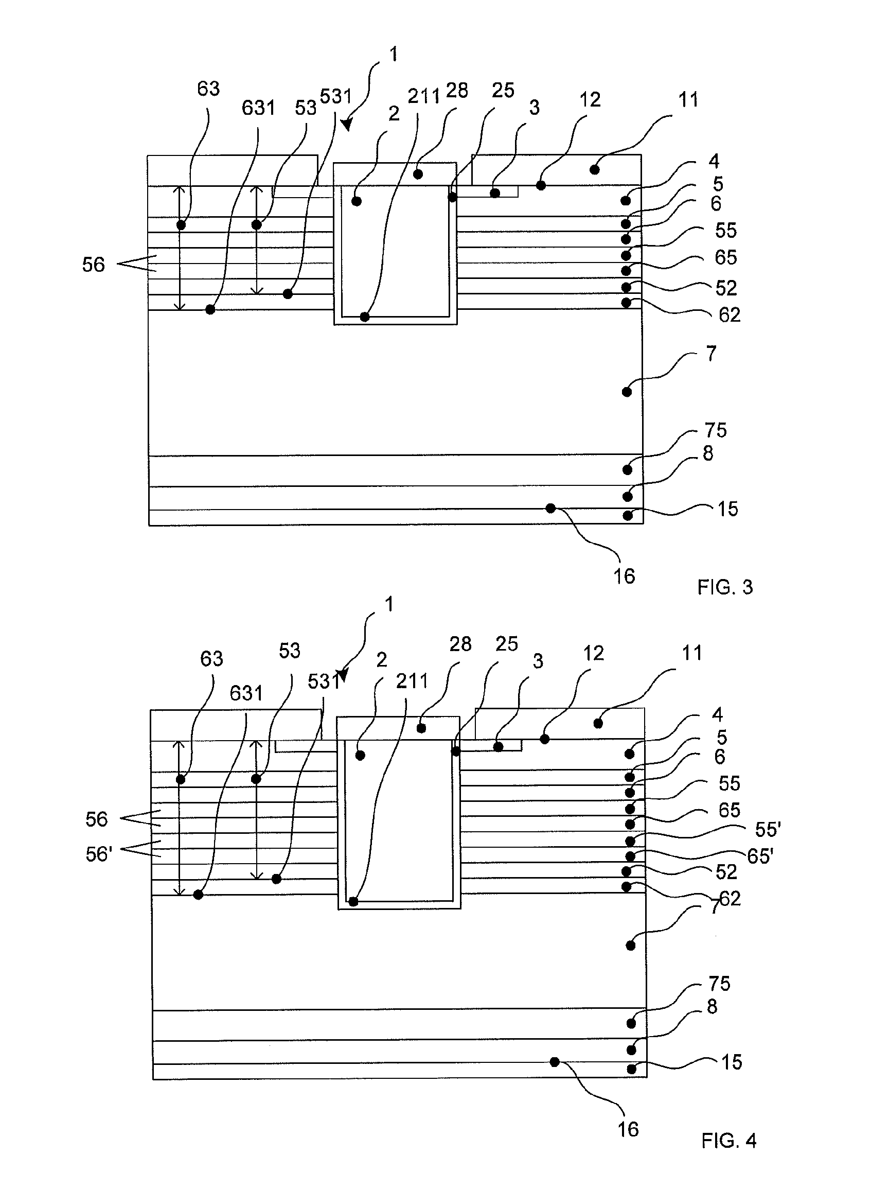
[0025]Exemplary embodiments of the present disclosure provide a bipolar power semiconductor device which overcomes the limitations of both trench EST and trench IGBT with respect to the trade-off between on-state voltage and collector current saturation (also referred to as short-circuit capability). For instance, exemplary embodiments of the present disclosure provide a device with low on-state voltage and current saturation at the same time.

[0026]An exemplary embodiment of the present disclosure provides a bipolar power semiconductor device which includes an emitter electrode and a gate electrode on an emitter side and a collector electrode on a collector side, respectively. The collector side lies opposite to the emitter side. The device has a structure with a plurality of layers of different conductivity types. The trench gate electrode and the layers are arranged in planes parallel to the emitter side each includes a bottom, which is arranged in a maximum distance, to which the...


PUM


Abstract

A bipolar power semiconductor device is provided with an emitter electrode on an emitter side and a collector electrode on a collector side. The device has a trench gate electrode and a structure with a plurality of layers of different conductivity types in the following order: at least one n doped source region, a p doped base layer, which surrounds the at least one source region, an n doped enhancement layer, a p doped additional well layer, an additional n doped enhancement layer, an additional p doped well layer, an n doped drift layer and a p doped collector layer. The trench gate electrode has a gate bottom, which is located closer to the collector side than the additional enhancement layer bottom.

Description

RELATED APPLICATION[0001]This application claims priority under 35 U.S.C. §119 to European Patent Application No. 10167819.1 filed in Europe on Jun. 30, 2010, the entire content of which is hereby incorporated by reference in its entirety.FIELD[0002]The present disclosure relates to the field of power electronics and more particularly to a power semiconductor device.BACKGROUND INFORMATION[0003]In the document “A dual gate emitter switched thyristor (DTG-EST) with dual trench gate electrode and different gate oxide thickness” by D. Kim et al, Microelectronic Engineering 70 (2003), pp. 50-57, a conventional emitter switched thyristor (EST) with a trench gate structure is described. With reference to FIG. 1, this EST is a bipolar power semiconductor device 1′ which includes an emitter electrode 11 on an emitter side 12 of a wafer, and a collector electrode 15 on a collector side 16 of the wafer. The collector side 16 lies opposite to the emitter side 12 on the wafer. The EST includes a...

Claims


Application Information

Patent Timeline
Patent Type & Authority Patents(United States)
IPC IPC(8): H01L27/118
CPCH01L29/7455H01L29/749H01L29/66712H01L29/7802
Inventor BAUER, FRIEDHELM
Owner HITACHI ENERGY SWITZERLAND AG
Why Eureka
Try Eureka