Suppression of row-wise noise in CMOS image sensors

a cmos image sensor and row-wise noise technology, applied in the field of image sensors, can solve the problems of correlated noise, non-correlated noise, horizontal stripes in the recreated, and single row pixel values are susceptible to and contain both correlated noise and non-correlated noise,

Active Publication Date: 2012-11-13
SEMICON COMPONENTS IND LLC
View PDF39 Cites 16 Cited by
  • Summary
  • Abstract
  • Description
  • Claims
  • Application Information

AI Technical Summary

Problems solved by technology

However, a consequence of row-wise sampling is that the pixel values from a single row are susceptible to and contain both correlated noise and non-correlated noise.
For example, noise on power supply and common bias lines are sources that will result in correlated noise.
When the correlated row noise component changes from row to row, an undesirable effect is likely to result in the form of horizontal stripes in the recreated image.
However, such approach will convert non-correlated noise from the dark reference pixels to row-wise noise.
Nevertheless, that may not be desirable or feasible for reasons such as limited die size and the need to minimize power consumption, just to name a few.

Method used


Image

  • Suppression of row-wise noise in CMOS image sensors
  • Suppression of row-wise noise in CMOS image sensors
  • Suppression of row-wise noise in CMOS image sensors

Examples


Embodiment Construction

[0019]Certain details are set forth below to provide a sufficient understanding of embodiments of the invention. However, it will be clear to one skilled in the art that embodiments of the invention may be practiced without these particular details. Moreover, the particular embodiments of the present invention described herein are provided by way of example and should not be used to limit the scope of the invention to these particular embodiments. In other instances, well-known circuits, control signals, and timing protocols have not been shown in detail in order to avoid unnecessarily obscuring the invention.

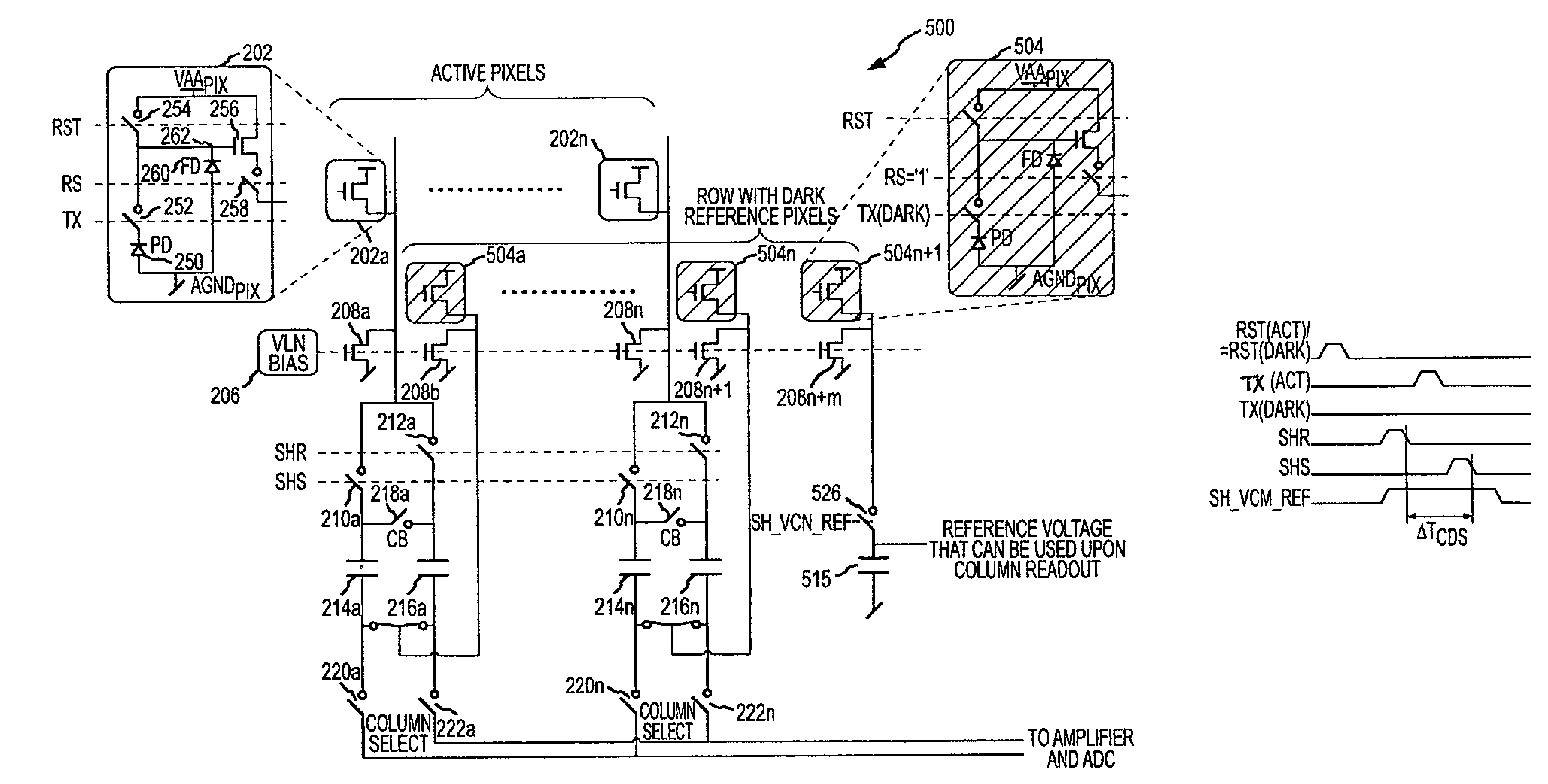
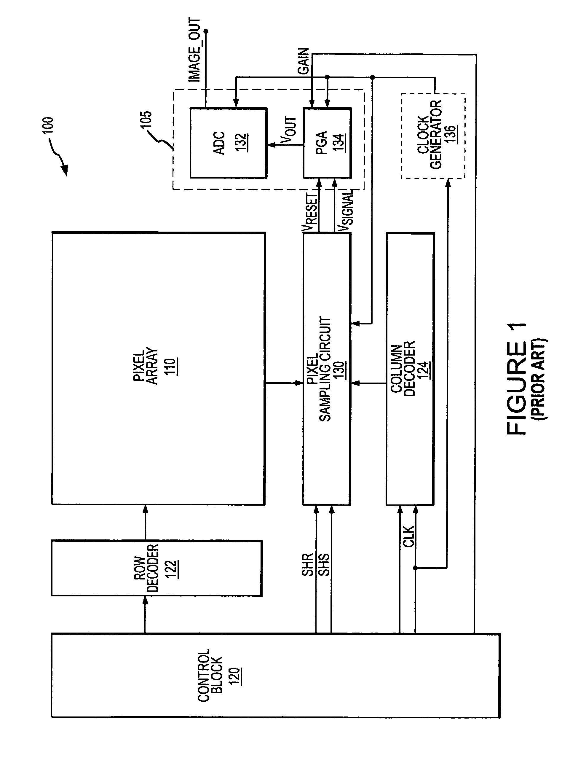
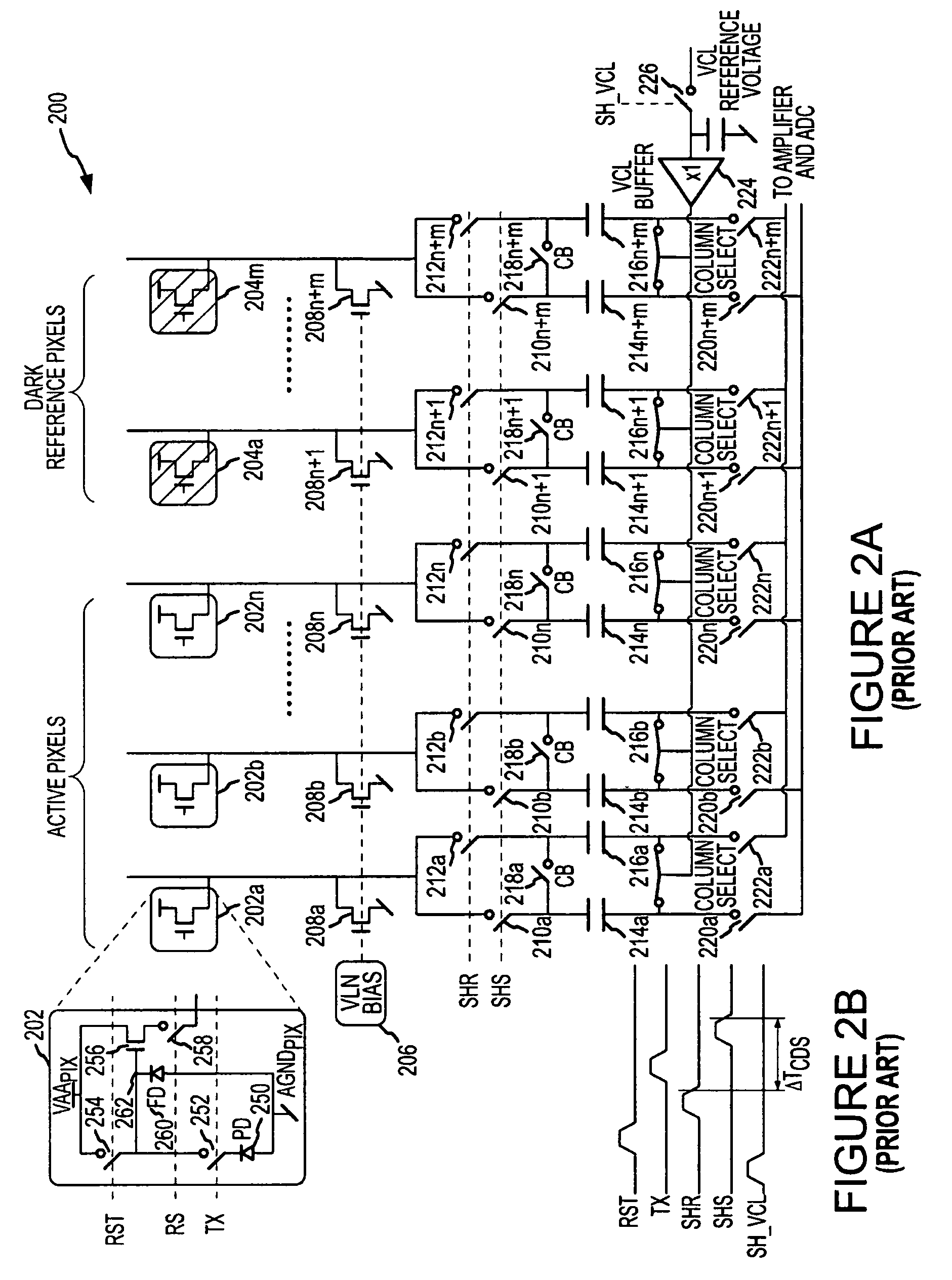
[0020]FIG. 1 illustrates a block diagram of a prior art CMOS image sensing device 100 having a pixel array 110 of light-sensing photosensors as previously described, or as implemented by other circuitry known in the art. A plurality of pixels arranged in rows and columns are respectively connected to a plurality of row and column lines that are provided for the entire array 110...


PUM


Abstract

Embodiments of circuits and methods for suppressing row-wise noise in the analog domain in an image sensing device. In one embodiment, a pixel sampling circuit includes a readout circuit that is connected to a plurality of pixels to receive analog signals from the pixels. The pixel sampling circuit also includes a noise correction circuit that provides a reference signal to remove at least a portion of the noise in the analog signals received from the pixels before the analog signals are converted into digital signals.

Description

TECHNICAL FIELD[0001]Embodiments of the present invention relate generally to image sensors, and more particularly, to noise suppression in image sensors.BACKGROUND OF THE INVENTION[0002]Complementary metal-oxide-semiconductor (CMOS) image sensors have in recent years been widely employed in image sensing applications such as digital cameras, video camcorders, scanners and the like. CMOS image sensors sense light by taking advantage of photoelectric effect. Photoelectric effect occurs when photons interact with crystallized silicon to energize and move electrons from the valence band into the conduction band, where the electrons can be harnessed, creating electric current at a voltage related to the bandgap energy. A conventional CMOS image sensor typically contains a focal plane array of light-sensing elements, referred to as picture elements or pixels, and readout circuitry that outputs signals indicative of the light sensed by the pixels. Each light-sensing element includes a pho...

Claims


Application Information

Patent Timeline
Patent Type & Authority Patents(United States)
IPC IPC(8): H04N5/217H04N9/64H04N5/335H01L27/00H04N3/14
CPCH04N3/1568H04N5/361H04N5/3658H04N5/3745H04N25/677H04N25/63H04N25/77H04N25/75
Inventor WILLASSEN, TRYGVE
Owner SEMICON COMPONENTS IND LLC
Why Eureka
Try Eureka