Eureka AIR delivers breakthrough ideas for toughest innovation challenges, trusted by R&D personnel around the world.

CMOS three-dimensional image sensor detectors with assured non collection of late arriving charge, more rapid collection of other charge, and with improved modulation contrast

a three-dimensional image sensor and detector technology, applied in the field of three-dimensional image sensor detectors, can solve the problems of shortened lifetime photocharges, degrade the accuracy and quality of presently acquired depth image data, and shorten the lifetime of photocharges, so as to maximize minimize the collection of photocharges, and maximize the collection of substantially all photocharges

Inactive Publication Date: 2012-11-20
MICROSOFT TECH LICENSING LLC
View PDF3 Cites 25 Cited by
  • Summary
  • Abstract
  • Description
  • Claims
  • Application Information

AI Technical Summary

Benefits of technology

[0030]The present invention recognizes that it can be counterproductive to simply maximize photocharge collection in a CMOS detector used in a three-dimensional TOF system. Simply stated, it is better to disregard late arriving photocharge, e.g., photocharge that arrives later for collection at the detector than faster arriving photocharge, than to allow such charge to contribute to the depth image produced by the TOF system. Thus, the present invention maximizes collection of substantially all photocharges whose creation time can be ascertained accurately, and minimizes collection of photocharges whose creation time cannot be ascertained accurately. Photocharges in the first category are charges that can be rapidly collected at the sensor collection region and will contribute meaningfully to the presently acquired depth image data. The creation time of such charges is reasonably known because the charges were created relatively near upper regions of the sensor semiconductor structure. However photocharges in the second category are charges that would arrive at the sensor collection region too late to meaningfully contribute to the presently acquired depth image data. These charges will have been created relatively deep within the sensor semiconductor structure, hence the longer time needed for them to reach a collection region, and uncertainty as to their time of creation. The rapidly collected charges represent accurate information as to the presently acquired depth image data, whereas the late arriving charges represent older depth image data that, if allowed to contribute to a depth image, would degrade the accuracy and quality of the presently acquired depth image data. Thus one aspect of the present invention enhances efficiency and accuracy of depth image data acquired by a TOF system by maximizing detection of useful (promptly arriving) charges, while minimizing detection of non-useful (late arriving) charges.
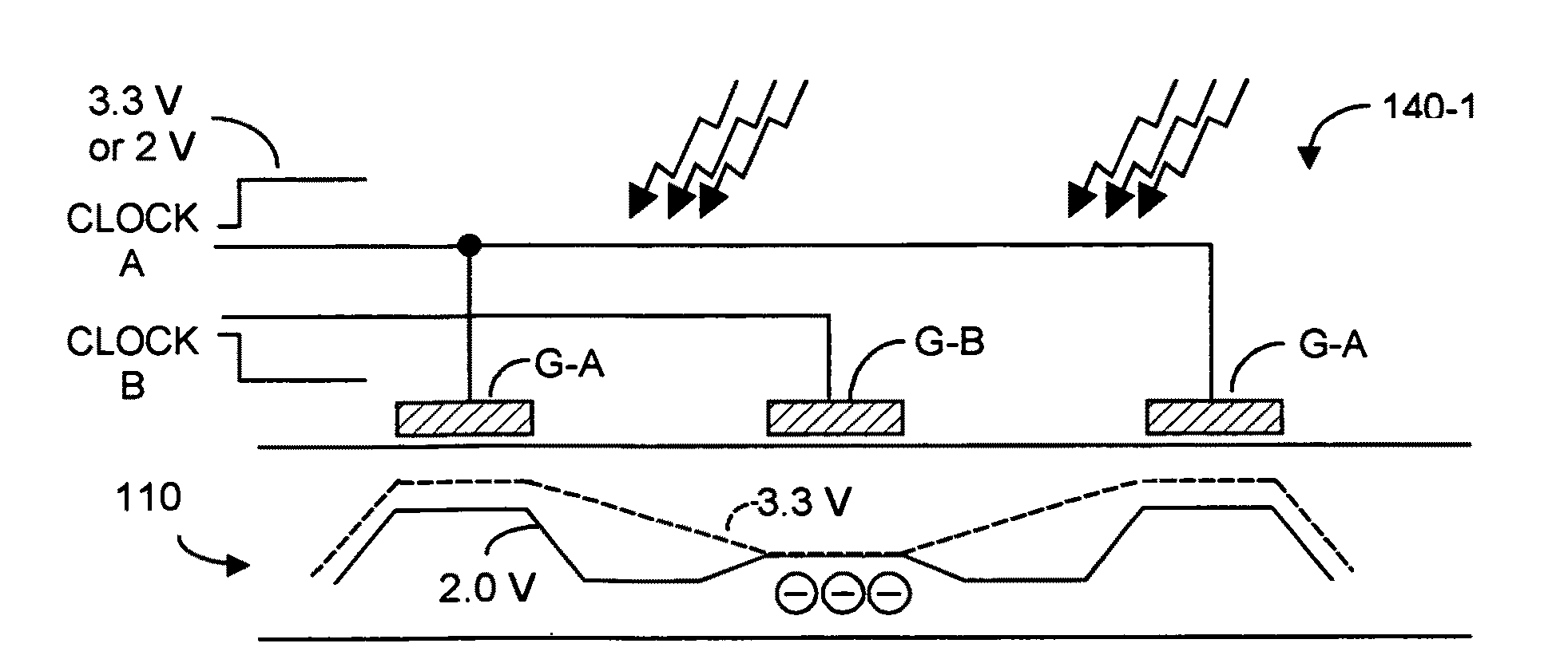
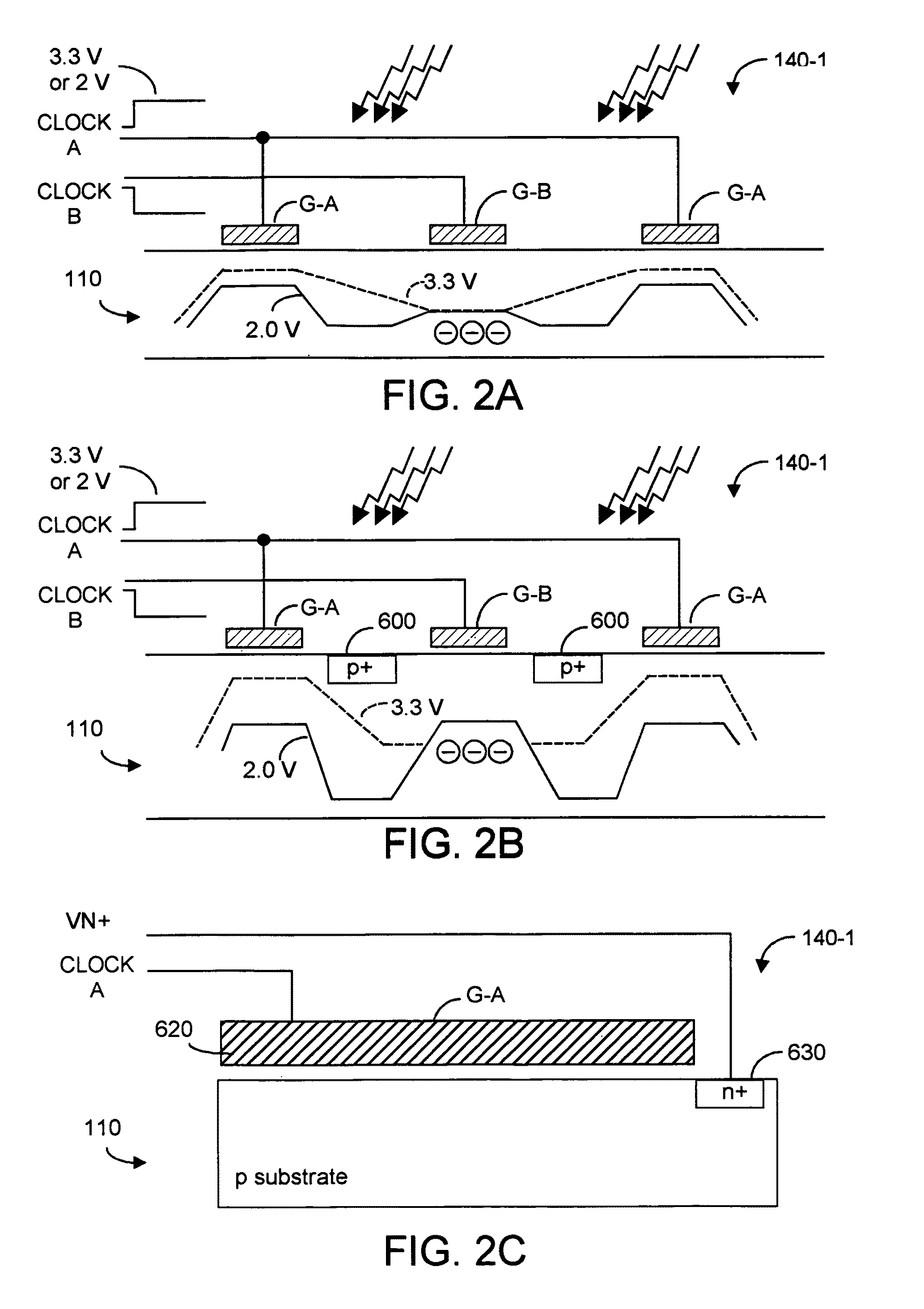
[0031]CMOS detectors in sophisticated TOF systems employ differential pixel detectors such that two collection regions (A and B) exist per pixel. Incoming optical energy, e.g., S2, generates photocharge within the pixel sensor semiconductor structure, which charges are collected at the A or B regions according to phase of the S2 signal. Photocharges whose arrival time can be ascertained accurately, e.g., promptly arriving charges, are quickly assigned to an arrival time interval. Preferably this is accomplished by applying voltages at the surface of the silicon substrate upon which the array of pixel photodetectors is fabricated. These voltages create a strong drift field that steers charge toward the correct A or B collection region. Doping gradients create additional drift fields to urge or move the charge into a substrate region within which the voltage created drift fields can take over. Preferably photocharges whose creation time cannot be ascertained accurately are minimized by exposing these charges to high doping levels, to shorten their lifetime. Consequently such shortened lifetime photocharges do not survive long enough to be exposed to drift fields and be moved towards collection areas. In embodiments, electric field barriers are created in the silicon substrate to impede movement of such photocharges towards the collection areas. Thus, there is a maximization of collected charges whose charge creation time is known with certainty, and a minimization of collection of other charges.
[0032]Embodiments of the present invention can be used with phase-based and non-phase-based TOF system detectors. In one aspect, embodiments of the present invention provide in the bottommost portion of the upper epitaxial collection region of interest a layer of epitaxy (epi) having a dopant concentration higher than the substrate. This highest dopant layer creates a barrier that prevents charge generated more deeply into the substrate from moving upward to be collected, such charge deemed late-arriving charge. In another aspect, embodiments of the present invention provide stratified regions of differently doped epitaxy within the upper epitaxial collection region of interest. Preferably each such layer is more lightly doped than the layer beneath it, and each of these layers is less heavily doped than the substrate. The electric field created by these strata of dopant gradient attract nearby charge (e.g., charge collected within the lower epitaxial collection region of interest) and urge the charge upward toward the next less heavily doped upper layer. CMOS detectors may employ one or more aspects of the present invention, to enhance quality of the acquired depth data, and to enhance AC modulation contrast. In another aspect of the present invention, the topmost layer of epitaxy is lightly doped to better enable the electric field resulting from overlying preferably elongated finger-like gates to further hasten charge collection.

Problems solved by technology

However photocharges in the second category are charges that would arrive at the sensor collection region too late to meaningfully contribute to the presently acquired depth image data.
These charges will have been created relatively deep within the sensor semiconductor structure, hence the longer time needed for them to reach a collection region, and uncertainty as to their time of creation.
The rapidly collected charges represent accurate information as to the presently acquired depth image data, whereas the late arriving charges represent older depth image data that, if allowed to contribute to a depth image, would degrade the accuracy and quality of the presently acquired depth image data.
Consequently such shortened lifetime photocharges do not survive long enough to be exposed to drift fields and be moved towards collection areas.

Method used


Image

  • CMOS three-dimensional image sensor detectors with assured non collection of late arriving charge, more rapid collection of other charge, and with improved modulation contrast
  • CMOS three-dimensional image sensor detectors with assured non collection of late arriving charge, more rapid collection of other charge, and with improved modulation contrast
  • CMOS three-dimensional image sensor detectors with assured non collection of late arriving charge, more rapid collection of other charge, and with improved modulation contrast

Examples


Embodiment Construction

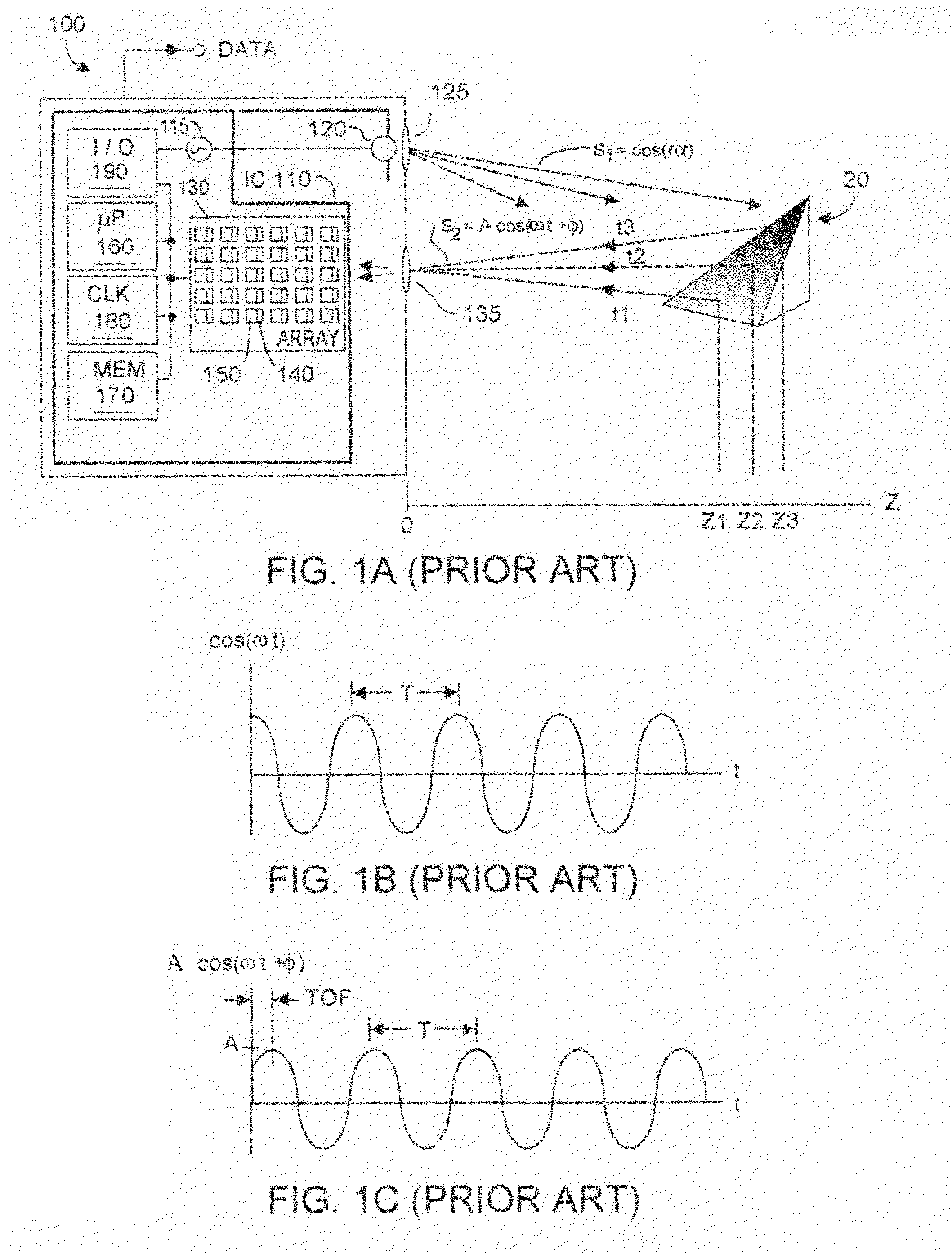
[0051]Embodiments of the present invention may be practiced with phase-based TOF systems such as depicted in FIG. 1A as exemplified by numerous U.S. patents to Canesta, Inc., including U.S. Pat. No. 7,352,454 (2008) or with non-phase based systems, e.g., as described in U.S. Pat. No. 6,323,942 (2001), assigned to Canesta, Inc. Embodiments of the present invention to improve collection of photocharge whose creation time is known, and to impede collection of photocharge whose creation time is not known (i.e., late arriving charge) can be implemented by modifying the structure of sensors 140 in FIG. 1A. Of course the present invention may be used with other sensors and may be used in non-TOF applications.

[0052]Sensors as described with respect to FIG. 1A, modeled on the '454 patent, thus are a good starting point. To recapitulate the description of the '454 sensors, the sensor structures included finger-shaped gate structures that extended along a y-axis, and were spaced-apart from eac...


PUM


Abstract

A CMOS-implementable TOF detector promptly collects charge whose creation time can be precisely known, while rejecting collection of potentially late arriving charge whose creation time may not be precisely known. Charges created in upper regions of the detector structure are ensured to be rapidly collected, while charges created in the lower regions of the detector structure, potentially late arriving charges, are inhibiting from being collected.

Description

CROSS-REFERENCE TO CO-PENDING APPLICATION[0001]Priority is claimed from applicants' U.S. provisional patent application Ser. No. 61 / 207,970, filed 17 Feb. 2009, and assigned to Canesta, Inc., of Sunnyvale, Calif., assignee herein.BACKGROUND OF THE INVENTION[0002]The invention relates generally to CMOS-implementable image sensors suitable for three-dimensional applications including time-of-flight (TOF) and phase-based TOF range or depth systems. More specifically, the invention concerns improving quality of acquired depth data by assuring non-collection of late arriving charges, and to shortening the collection time for remaining charges.[0003]Ordinary color cameras have a sensor that comprises an array of color pixels that acquire a two-dimensional image of a scene, for which each pixel produces a color value. A black and white camera has an array whose pixels produce gray scale values. Incoming light (photon energy) from the scene falls upon the color or gray scale pixel array and...

Claims


Application Information

Patent Timeline
Patent Type & Authority Patents(United States)
IPC IPC(8): G01C3/08
CPCG01S7/4816G01S17/89H04N5/37452H01L27/14609G01S17/894H04N25/771
Inventor BAMJI, CYRUSMEHTA, SWATIELKHATIB, TAMER AHMED TAHA
Owner MICROSOFT TECH LICENSING LLC
Why Eureka
Eureka Blog
Learn More