Rib reinforcement of plated thru-holes

a technology of rib reinforcement and thru-hole, which is applied in the field of rib reinforcement of plated thru-hole, can solve the problems of limiting the available routing area of signal traces on layers immediately, requiring much more layout effort and higher initial cost than either wire, and reducing the likelihood of pth damage, etc., to reduce the heat sinking effect of pths, the effect of high reliability and reworkability

Active Publication Date: 2012-11-27
ORACLE INT CORP
View PDF1 Cites 6 Cited by
  • Summary
  • Abstract
  • Description
  • Claims
  • Application Information

AI Technical Summary

Benefits of technology

[0016]The present embodiments provide methods and systems for providing improved mechanical support for plated through-holes (PTH) in PCBs, which advantageously allows the PCBs to exhibit high reliability and reworkability. Such methods and systems are achieved by providing one or more electrically-nonfunctional (or unused) lands on one or more internal layers surrounding the PTHs. In this regard, the unused lands act as “anchors” to the outer walls of the PTHs, thereby reducing the likelihood that the PTHs will be damaged during assembly and / or rework processes. These “anchors” are also referred to as “ribs.” Additionally, the heat sinking effects of PTHs may be reduced by providing one or more vias surrounding the PTHs to provide an electrical connection between the PTH and the bottom layer of a PCB, thereby improving the soldering capabilities of the PTHs. In this regard, the PTHs may not directly contact all of the internal ground or power layers, so the heat sinking or heat transfer effects are reduced. This feature enables molten solder to fill substantially the entire PTH before freezing. Further, one or more of the surrounding vias may be coupled to some or all of the ground or power layers without substantially increasing the heat sinking or transfer effects of the PTH. Various features and embodiments of the present invention are described in detail below.
[0017]According to a first aspect of the present invention, a multi-layer printed circuit board (PCB) is provided. The PCB includes a plurality of conductive layers with dielectric material disposed therebetween. Further, the PCB includes a plated through-hole that extends through the PCB, the plated through-hole including a conductive lining that forms a barrel. The PCB also includes a via, spaced apart from the plated through-hole, electrically coupled to one or more internal conductive layers of the plurality of conductive layers. Additionally, the plated through-hole is electrically coupled to the via, and the plated through-hole is spaced apart from at least one of the one or more internal conductive layers. The PCB further includes an electrically-nonfunctional land formed in one of the plurality of conductive layers. In addition, the electrically-nonfunctional land is in contact with an outer wall of the barrel of the plated through-hole. In this manner, the electrically-nonfunctional land provides improved mechanical support the plated through-hole (PTH), which advantageously allows the PCB to exhibit high reliability and reworkability.

Problems solved by technology

They require much more layout effort and higher initial cost than either wire-wrapped or point-to-point constructed circuits, but are much cheaper and faster for high-volume production.
While through-hole mounting provides strong electrical and mechanical bonds when compared to surface-mount technology techniques, the additional drilling required makes the boards more expensive to produce.
They also limit the available routing area for signal traces on layers immediately below the top layer on multilayer boards since the holes must pass through all layers to the opposite side.
Too little flux will cause poor joints, while too much flux may cause cosmetic or other problems.
As the thickness of a PCB increases (e.g., above 100 mils, 150 mils, 200 mils, or more) and the mass of copper sheets increases (e.g., above 0.5 oz, 1.0 oz, 1.5 oz, 2.0 oz, or more), it may become more difficult to successfully fill the pin holes during the soldering process.
One cause of the increased difficulty is that the molten solder tends to cool (“freeze”) prematurely before it has traveled from the bottom of the PCB to the top.
The multiple layers of copper sheets may conduct heat away from the molten solder (i.e., act as heat sinks), causing the solder to freeze prematurely and causing the pin hole to be only partially filled with solder (e.g., 75% filled, 50% filled, or less).
When the pin hole is only partially filled with solder, the mechanical and electrical integrity of the solder connection may be significantly reduced or may even be ineffective.

Method used


Image

  • Rib reinforcement of plated thru-holes
  • Rib reinforcement of plated thru-holes
  • Rib reinforcement of plated thru-holes

Examples


Embodiment Construction

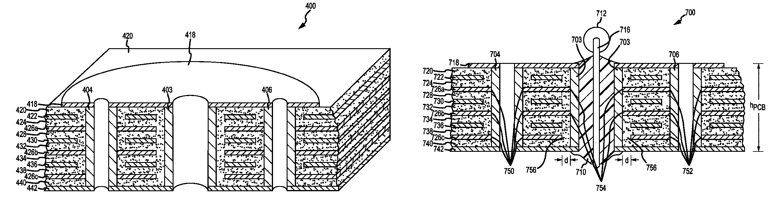
[0031]The present embodiments provide methods and systems for providing improved mechanical support for plated through-holes (PTH) in PCBs, which advantageously allows the PCBs to exhibit high reliability and reworkability. Such methods and systems are achieved by providing one or more electrically-nonfunctional (or unused) lands on one or more internal layers surrounding the PTHs. In this regard, the unused lands act as “anchors” to the outer walls of the PTHs, thereby reducing the likelihood that the PTHs will be damaged during assembly and / or rework processes. Additionally, the heat sinking effects of PTHs may be reduced by providing one or more vias surrounding the PTHs to provide an electrical connection between the PTH and the bottom layer of a PCB, thereby improving the soldering capabilities of the PTHs. In this regard, the PTHs may not directly contact all of the internal ground or power layers, so the heat sinking or heat transfer effects are reduced. This feature enables ...


PUM

PropertyMeasurementUnit
thicknessaaaaaaaaaa
thicknessaaaaaaaaaa
thicknessaaaaaaaaaa

Abstract

Systems and methods for providing mechanically reinforced plated through-holes (PTH) in PCBs, which advantageously allow improved soldering capabilities and reliability, are described herein. Such systems and methods are achieved by reducing the heat sinking effects of PTHs by providing one or more vias surrounding the PTHs to provide an electrical connection between the PTH and the internal and bottom conductive layers of a PCB. In this regard, the PTHs are spaced apart from at least one of the internal conductive layers (e.g., ground or power layers), so the heat sinking effects are reduced. This feature enables molten solder to substantially fill the entire PTH before freezing, thereby improving the mechanical and electrical connection between an electrical component and the PCB. One or more electrically-nonfunctional lands (or “rib reinforcements”) are provided in internal conductive layers to mechanically support the walls of the PCB. These rib reinforcements improve the mechanical strength of the PTHs without affecting the electrical performance and without impacting the ability to solder components to the PCB.

Description

BACKGROUND OF THE INVENTION[0001]Printed circuit boards, or PCBs, are generally used to mechanically support and electrically connect electronic components using conductive pathways, or traces etched from copper sheets laminated onto a non-conductive substrate. A PCB populated with electronic components is referred to as a printed circuit assembly (PCA), also known as a printed circuit board assembly (PCBA). PCBs are generally rugged, inexpensive, and can be highly reliable. They require much more layout effort and higher initial cost than either wire-wrapped or point-to-point constructed circuits, but are much cheaper and faster for high-volume production. Some PCBs have trace layers inside the PCB and are called multi-layer PCBs, and may be formed by bonding together separately etched thin boards. Some multi-layer PCBs may include several layers (e.g., 4 layers, 12 layers, 24 layers, or more).[0002]Holes are typically drilled through a PCB with tiny drill bits (e.g., made of solid...

Claims


Application Information

Patent Timeline
Patent Type & Authority Patents(United States)
IPC IPC(8): H05K1/11
CPCH05K1/116H05K3/3447H05K3/429H05K2201/062Y10T29/49142H05K2201/09454H05K2201/09627H05K2201/09781Y10T29/49124H05K2201/09309
Inventor MARTINEZ-VARGAS, JORGE EDUARDOHU, LIEN-FEN LIVIALEE, SAMUEL MING SIENBRITTON, JAMES DAVIDHENSON, MARTIN JOHN
Owner ORACLE INT CORP
Why Eureka
Try Eureka