Method and system of embedded microlens

a technology of embedded microlens and microlens, which is applied in the direction of radio frequency controlled devices, semiconductor devices, electrical apparatus, etc., can solve the problems of non-standard packaging methods, difficult to reduce the size of devices, and the cost of ic fabrication facilities can be hundreds of millions or even billions of dollars, so as to reduce the processing steps of photolithography, reduce the processing cost, and facilitate the use

Active Publication Date: 2012-11-27
SEMICON MFG INT (SHANGHAI) CORP
View PDF9 Cites 7 Cited by
  • Summary
  • Abstract
  • Description
  • Claims
  • Application Information

AI Technical Summary

Benefits of technology

[0012]Embodiments of the present invention provide many benefits over conventional techniques. For example, embodiments of the present invention provide an easy to use process that is much simplified with less processing steps in photolithography and polishing and is thus more cost effective than the conventional microlens fabrication process. In some embodiments, the present invention provides a method for forming the microlens that does not depend on thermal curing. A wide variety of lens materials, instead of a limited selection of lens materials suitable for low-temperature processing in conventional art, allows a flexible choice of packaging, including those designed for high-temperature soldering. Additionally, the present invention provides an improved microlens design using a dry-wet combination etching in addition to a chemical-mechanical planarization process to enhance the performance of an imaging sensor. The novel truncated plano-convex shape of the microlens and the short distance between the microlens and the photo sensing region help to alleviate oblique light beam problems. Moreover, embodiments of the present invention provide a process that can be integrated in the established silicon wafer back-end-of-line (BEOL) processing. In a specific embodiment, the integrated microlens fabrication can be particularly useful for contact image sensor (CIS) applications. Depending upon the embodiment, one or more of these benefits may be achieved. These and other benefits will be described in more details throughout the present specification and more particularly below.

Problems solved by technology

An IC fabrication facility can cost hundreds of millions, or even billions, of dollars.
Making devices smaller is very challenging, as each process used in IC fabrication has a limit.
This conventional approach, wherein microlenses are formed on top of the color filters, requires separate material and lithography processing, and non-standard packaging methods due to the existence of an air gap for facilitating proper focusing of incident light beams.
The low temperature process may limit the use of the microlenses in high-temperature soldering applications.

Method used


Image

  • Method and system of embedded microlens
  • Method and system of embedded microlens
  • Method and system of embedded microlens

Examples


Embodiment Construction

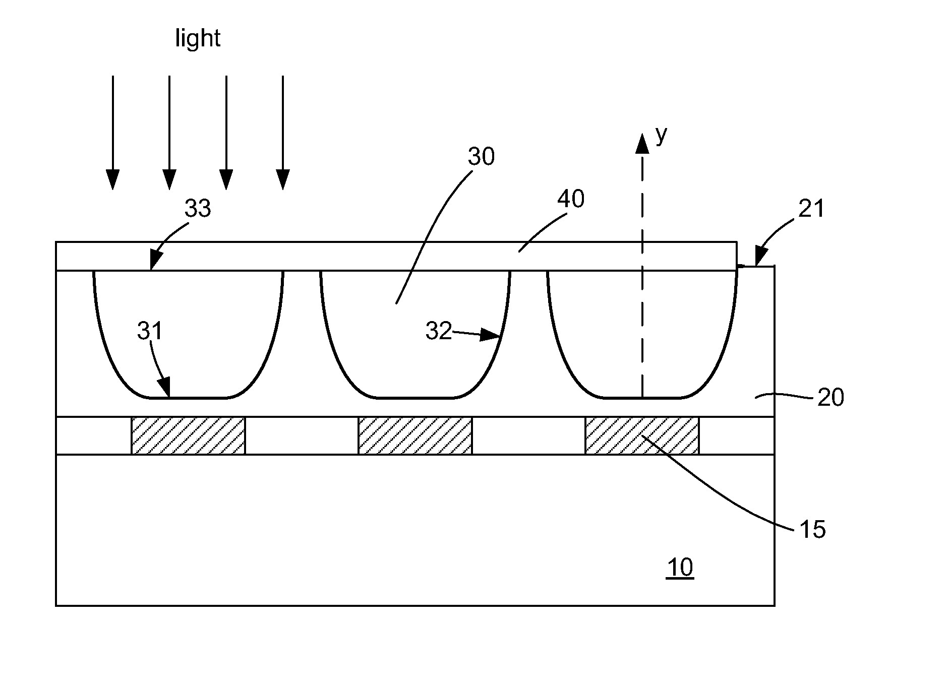
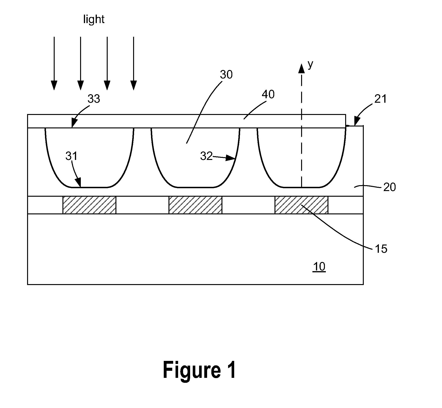
[0018]Embodiments of the present invention relate to integrated circuits and the processing for the manufacture of semiconductor devices. More particularly, embodiments of the present invention provide methods and structures for making an embedded microlens for integrated photo-electronic devices. But it would be recognized that the invention has a much broader range of applicability. For example, embodiments of the present invention can be applied to a variety of charge-coupled devices and CMOS image sensors containing microlens and contact image sensor (CIS) applications.

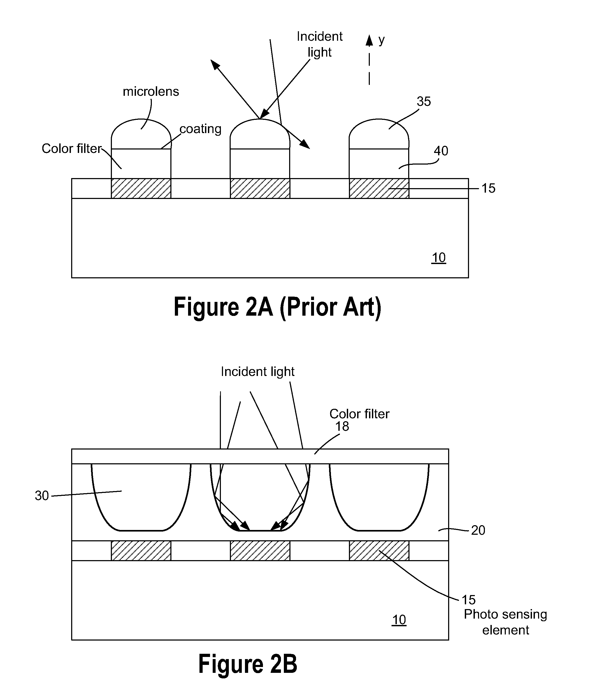
[0019]A conventional microlens fabrication process is often performed after the silicon processing or on a finished silicon wafer. Typically, microlenses are formed after the formation of color filters. The conventional process requires that a coating material be applied on the color filter layer and that the coating material be planarized prior to the deposition of the lens material. Multiple separate photolithog...


PUM


Abstract

An image sensor includes an array of photo-sensing regions formed in a semiconductor substrate, a dielectric layer over the array of photo-sensing regions, and an array of microlenses formed in the dielectric layer. Each of the microlenses is center-aligned over one of the photo-sensing regions and has a truncated plano-convex shape. The microlenses have an index of refraction that is higher than the dielectric layer's refraction index. Each of the microlenses has a smooth circular top, a flat circular bottom, and a curved circumferential side convex towards the semiconductor substrate.

Description

CROSS-REFERENCES TO RELATED APPLICATIONS[0001]This application claims priority to Chinese Patent Application No. 201010022718.2, filed Jan. 12, 2010, which is commonly owned and incorporated by reference herein for all purposes.BACKGROUND OF THE INVENTION[0002]Embodiments of the present invention relate to integrated circuits and the processing for the manufacture of semiconductor devices. More particularly, embodiments of the present invention provide structures of an embedded microlens that can be made and packaged easily and methods for making such structures. The microlens according to embodiments of the present invention can be applied to charge-coupled devices (CCDs), color CMOS image sensors, contact image sensors, and others. But it would be recognized that the invention has a much broader range of applicability. For example, the invention can be applied to make a variety of photometric devices and distance measuring devices containing microlens to increase the amount of lig...

Claims


Application Information

Patent Timeline
Patent Type & Authority Patents(United States)
IPC IPC(8): H01L31/0232
CPCH01L27/14627H01L27/14685
Inventor YANG, JIANPINGHUANG, HERBHUO, JIEGUANG
Owner SEMICON MFG INT (SHANGHAI) CORP
Why Eureka
Try Eureka