Phase-shift mask with assist phase regions
a phase region and mask technology, applied in the field of phase shift masks, can solve the problems of not all manufacturing applications have this flexibility, feature patterns formed adjacent to the field edge tend to be distorted, and conventional alternating phase phase shift masks cannot be employed, so as to increase the amount of light emitted
- Summary
- Abstract
- Description
- Claims
- Application Information
AI Technical Summary
Benefits of technology
Problems solved by technology
Method used
Image
Examples
example phase-shift masks
[0062]FIG. 8A is a schematic diagram of a portion of an example phase-shift mask 112 where phase-shift mask pattern 115 comprises transmissive phase-shift features or regions R, with transmissive phase-shift regions R0 having a 0° phase shift and transmissive phase-shift regions Rπ having a 180° (π) phase shift.
[0063]FIG. 8B is a close-up view of four phase-shift regions R of phase-shift mask 112 of FIG. 8A. Phase-shift regions R0 and Rπ are square with a dimension (side length) L, with the phase-shift regions R having equal area and configured in a checkerboard pattern or array. In an example embodiment, phase-shift regions R can have any reasonable shape, and in particular can have at least one of a circular shape, oval shape and a polygonal shape.
[0064]Photolithography system 100, when configured with phase-shift mask 112 having a checkerboard phase-shift mask pattern 115, can perform photolithographic imaging to form in photoresist layer 135 corresponding periodic (e.g., checker...
example method
for Forming the Roughened Substrate Surface
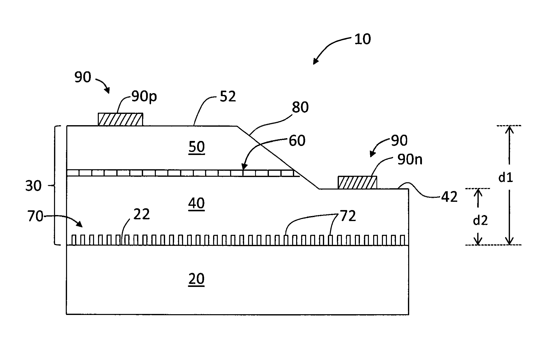
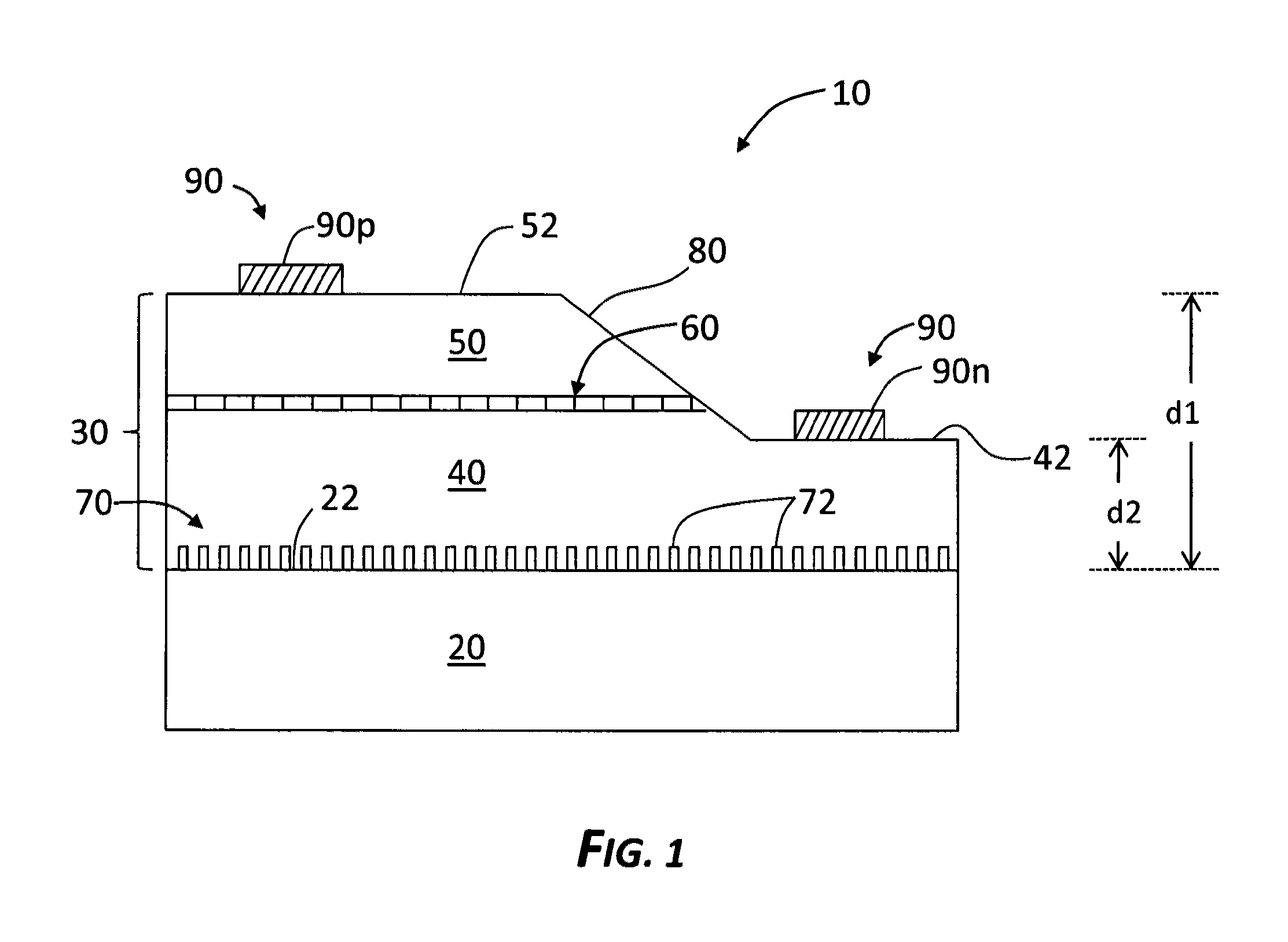
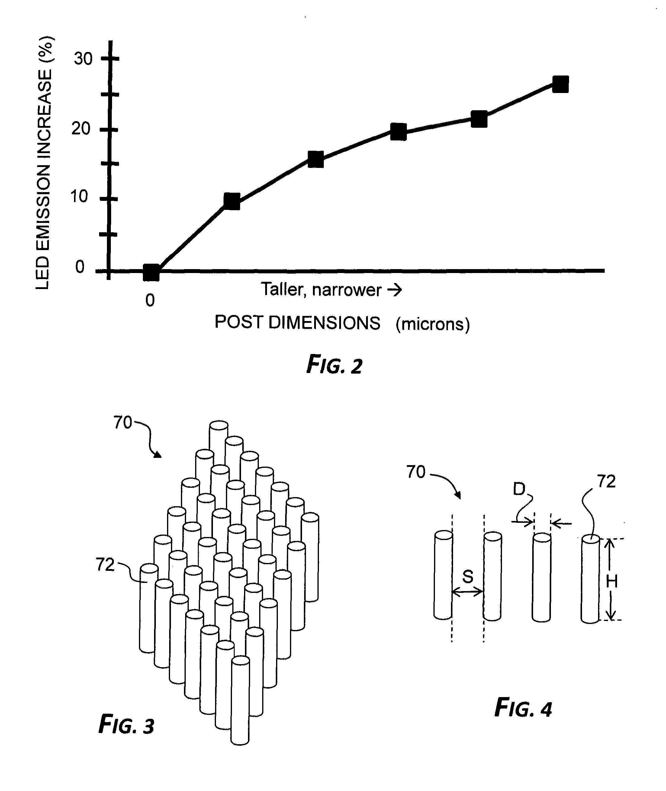
[0089]Thus, an aspect of the disclosure includes a method of forming a roughed substrate surface 22 having an array 70 of posts 72 in the course of forming LEDs 10 using photolithographic imaging and photolithographic processing techniques using phase-shift mask 112 with assist phase regions R′ as described above. An example method of forming array 70 of posts 72 is now described with reference to FIG. 6 and also to FIGS. 14A through 14E.
[0090]With reference first to FIG. 14A, the method includes providing a substrate 20 having photoresist layer 135 atop substrate surface 22. The method then includes arranging the coated substrate 20 on substrate stage 130 of photolithography system 100 (FIG. 6). The phase-shift mask 112 as described above (see, e.g., FIGS. 11A through 11C) that includes checkerboard array 115C and assist pattern 115A is arranged at mask stage 110 of photolithography system 100. The method then includes operating photolitho...
PUM
| Property | Measurement | Unit |
|---|---|---|
| wavelength | aaaaa | aaaaa |
| refractive index | aaaaa | aaaaa |
| thickness | aaaaa | aaaaa |
Abstract
Description
Claims
Application Information


