Surface-plasmon detector based on a field-effect transistor

a field-effect transistor and detector technology, applied in the field of surface-plasmon signal detectors, can solve the problem that the sp-signal detectors capable of appropriately responding to the full range of available modulation speeds are not yet sufficiently developed, and achieve the effect of small size and efficien

Active Publication Date: 2013-01-01
ALCATEL LUCENT SAS
View PDF28 Cites 5 Cited by
  • Summary
  • Abstract
  • Description
  • Claims
  • Application Information

AI Technical Summary

Benefits of technology

[0007]According to one embodiment, a surface-plasmon (SP) beam generated by an SP source and directed via an SP waveguide is applied to a gate node of a field-effect transistor (FET). The FET also has a source node and a drain node. In a representative configuration, the gate, source, and drain nodes are electrically biased to pass an electrical current between the source and drain nodes in a manner that makes the electrical current responsive to the intensity of the SP beam. Advantageously, the FET can serve as a relatively small and efficient SP-signal detector capable of responding to SP-beam modulation speeds as high as about 100 GHz, or even higher.

Problems solved by technology

However, SP-signal detectors capable of appropriately responding to the full range of available modulation speeds are not yet sufficiently developed.

Method used


Image

  • Surface-plasmon detector based on a field-effect transistor
  • Surface-plasmon detector based on a field-effect transistor
  • Surface-plasmon detector based on a field-effect transistor

Examples


Embodiment Construction

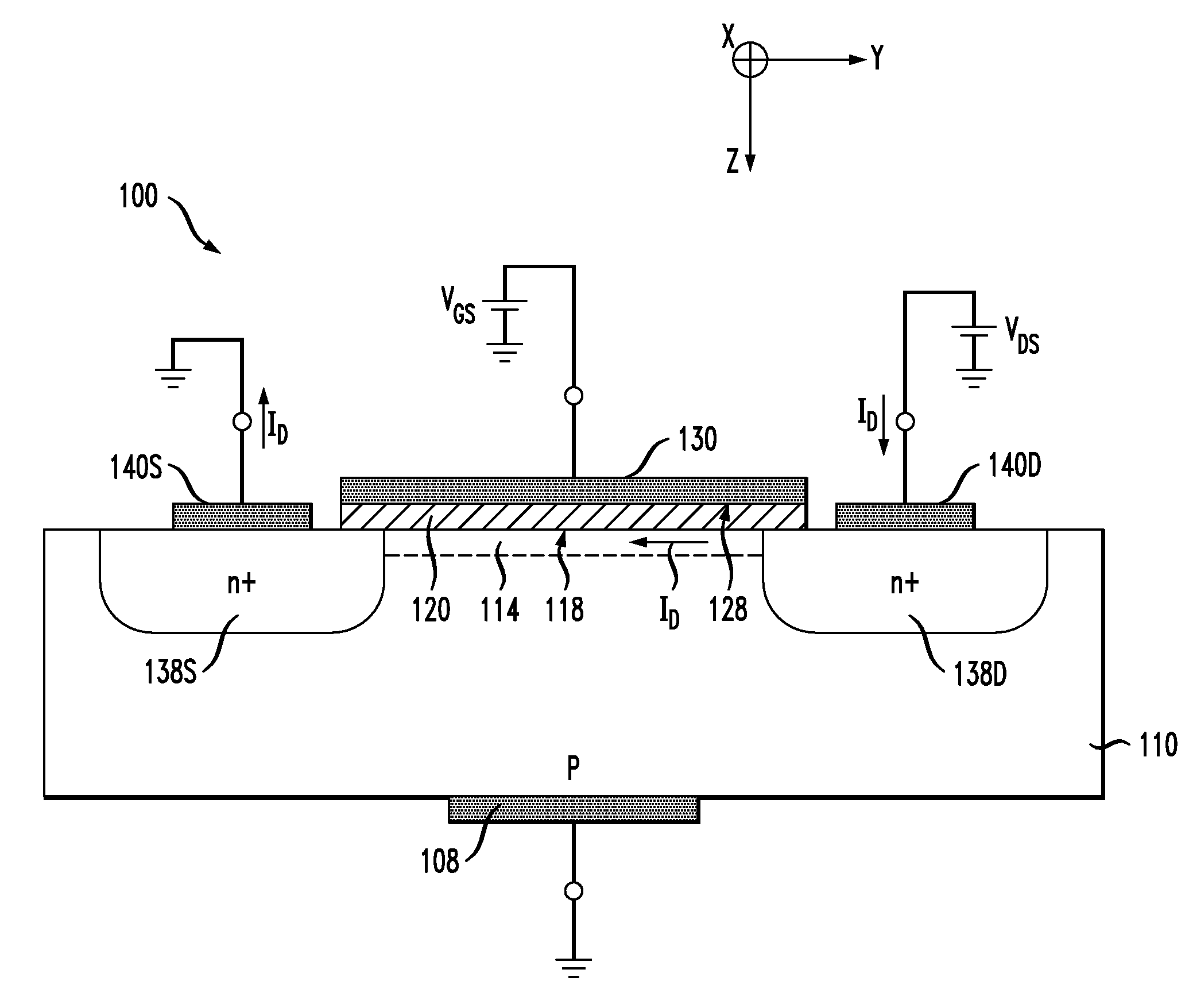
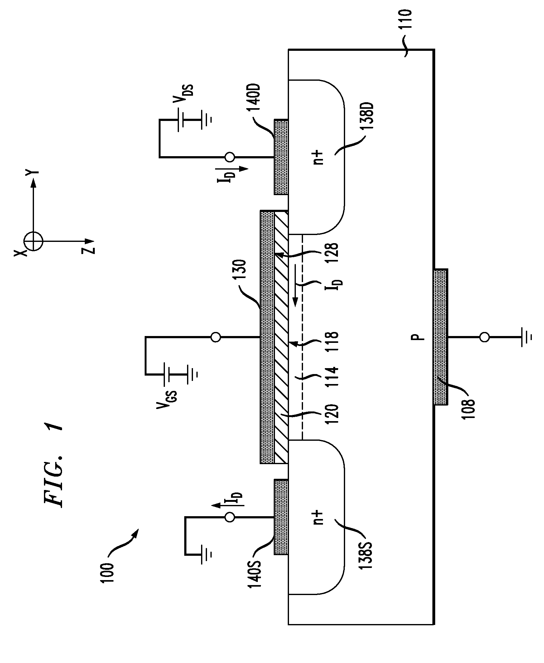
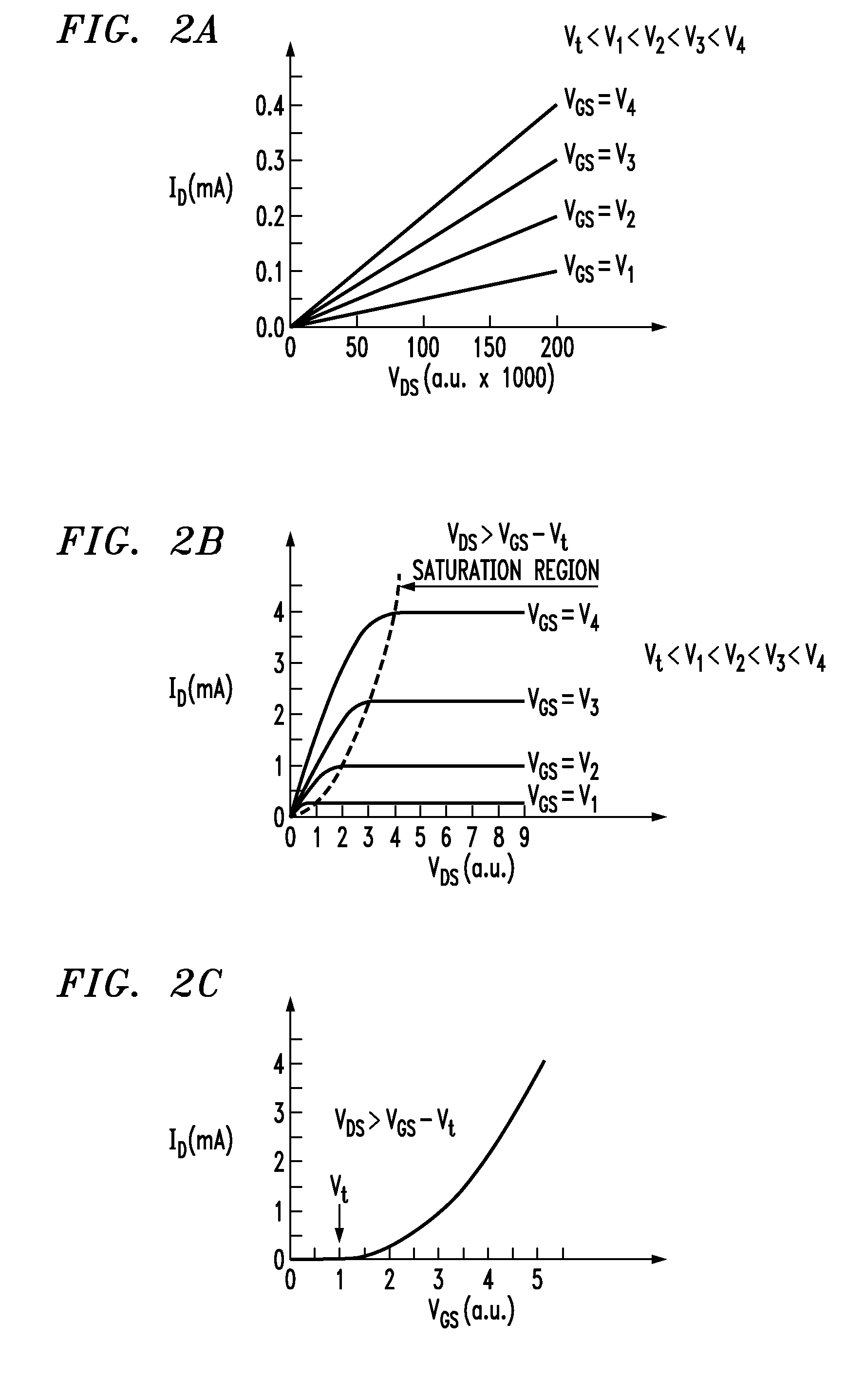
[0017]FIG. 1 shows a cross-sectional side view of a field-effect transistor (FET) 100 according to one embodiment of the invention. FIG. 1 also shows certain representative electrical connections, voltages, and currents that help to explain the operation of FET 100. As further detailed below, FET 100 can be configured using a prior-art method of operation and / or a method of operation according to one embodiment of the invention. These methods are described in reference to FIGS. 2A-C and FIG. 4, respectively.

[0018]In the embodiment of FIG. 1, FET 100 is an n-channel device. In an alternative embodiment, FET 100 can be a p-channel device. As known in the art, n- and p-channel FETs principally conduct through electrons and holes, respectively. While the description below primarily focuses on an n-channel FET, one of ordinary skill in the art will be able to use this description to derive a description applicable to a p-channel FET, e.g., by reversing the polarity of the voltages and cu...


PUM


Abstract

According to one embodiment, a surface-plasmon (SP) beam generated by an SP source and directed via an SP waveguide is applied to a gate node of a field-effect transistor (FET). The FET also has a source node and a drain node. In a representative configuration, the gate, source, and drain nodes are electrically biased to pass an electrical current between the source and drain nodes in a manner that makes the electrical current responsive to the intensity of the SP beam.

Description

BACKGROUND OF THE INVENTION[0001]1. Field of the Invention[0002]The present invention relates to electronic and / or plasmonic circuit elements and, more specifically, to surface-plasmon signal detectors.[0003]2. Description of the Related Art[0004]This section introduces aspects that may help facilitate a better understanding of the invention(s). Accordingly, the statements of this section are to be read in this light and are not to be understood as admissions about what is in the prior art and / or what is not in the prior art.[0005]Surface plasmons (SPs), also often referred to as surface-plasmon polaritons, are surface-bound waves that can propagate, e.g., along a metal-dielectric interface or along a metal-vacuum interface. An SP can be qualitatively viewed as a combination of an electromagnetic wave and an associated charge-density wave. The electromagnetic wave propagates along the interface due to its interaction with free surface charges of the metal. The interaction also cause...

Claims


Application Information

Patent Timeline
Patent Type & Authority Patents(United States)
IPC IPC(8): G01R31/02G01R31/26
CPCB82Y20/00G02B6/1226H01L31/1126
Inventor BLUMBERG, GIRSH
Owner ALCATEL LUCENT SAS
Why Eureka
Try Eureka