[0012]The resistance of the memory element, and thus its detectable storage state, can be repetitively set from an initial level to another level and then re-set back to the initial level. For some materials, the amount or duration of the voltage, current, electric field, heat and the like applied to change its state in one direction is different (asymmetrical) with that applied to change in another direction. With two detectable states, each memory element stores one-bit of data. With the use of some materials, more than one bit of data may be stored in each memory element by designating more than two stable levels of resistance as detectable states of the memory element. The three-dimensional array architecture herein is quite versatile in the way it may be operated.
[0013]This three-dimensional architecture also allows limiting the extent and number of unaddressed (non-selected) resistive memory elements across which an undesired level of voltage is applied during reading and programming operations conducted on other addressed (selected) memory elements. The risk of disturbing the states of unaddressed memory elements and the levels of leakage current passing through unaddressed elements may be significantly reduced from those experienced in other arrays using the same memory element material. Leakage currents are undesirable because they can alter the apparent currents being read from addressed memory elements, thereby making it difficult to accurately read the states of addressed (selected) memory elements. Leakage currents are also undesirable because they add to the overall power draw by an array and therefore undesirably causes the power supply to have to be made larger than is desirable. Because of the relatively small extent of unaddressed memory elements that have voltages applied during programming and reading of addressed memory elements, the array with the three-dimensional architecture herein may be made to include a much larger number of memory elements without introducing errors in reading and exceeding reasonable power supply capabilities.
[0014]In addition, the three-dimensional architecture herein allows variable resistance memory elements to be connected at preferably orthogonal crossings of bit and word line conductors without the need for diodes or other non-linear elements being connected in series with the variable resistive elements. In existing arrays of variable resistance memory elements, a diode is commonly connected in series with each memory element in order to reduce the leakage current though the element when it is unselected but nevertheless has a voltage difference placed across it, such as can occur when the unselected memory element is connected to a bit or word line carrying voltages to selected memory elements connected to those same lines. The absence of the need for diodes significantly reduces the complexity of the array and thus the number of processing steps required to manufacture it.
[0015]Indeed, the manufacture of the three-dimensional array of memory elements herein is much simpler than other three-dimensional arrays using the same type of memory elements. In particular, a fewer number of masks is required to form the elements of each plane of the array. The total number of processing steps needed to form integrated circuits with the three-dimensional array is thus reduced, as is the cost of the resulting integrated circuit.Double-Global-Bit-Line Architecture
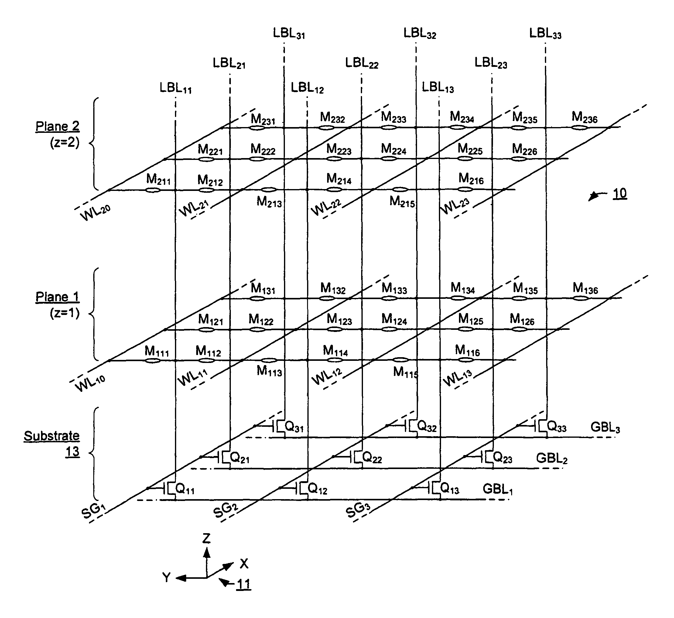
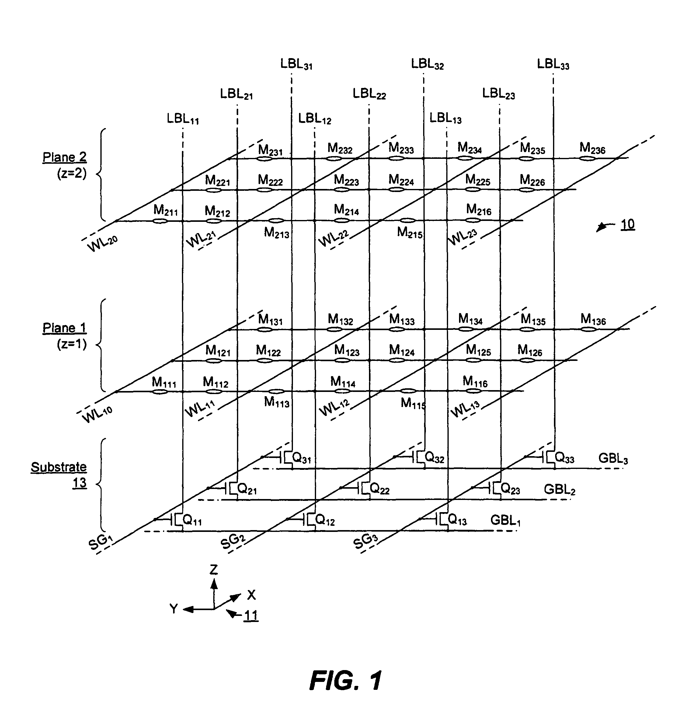
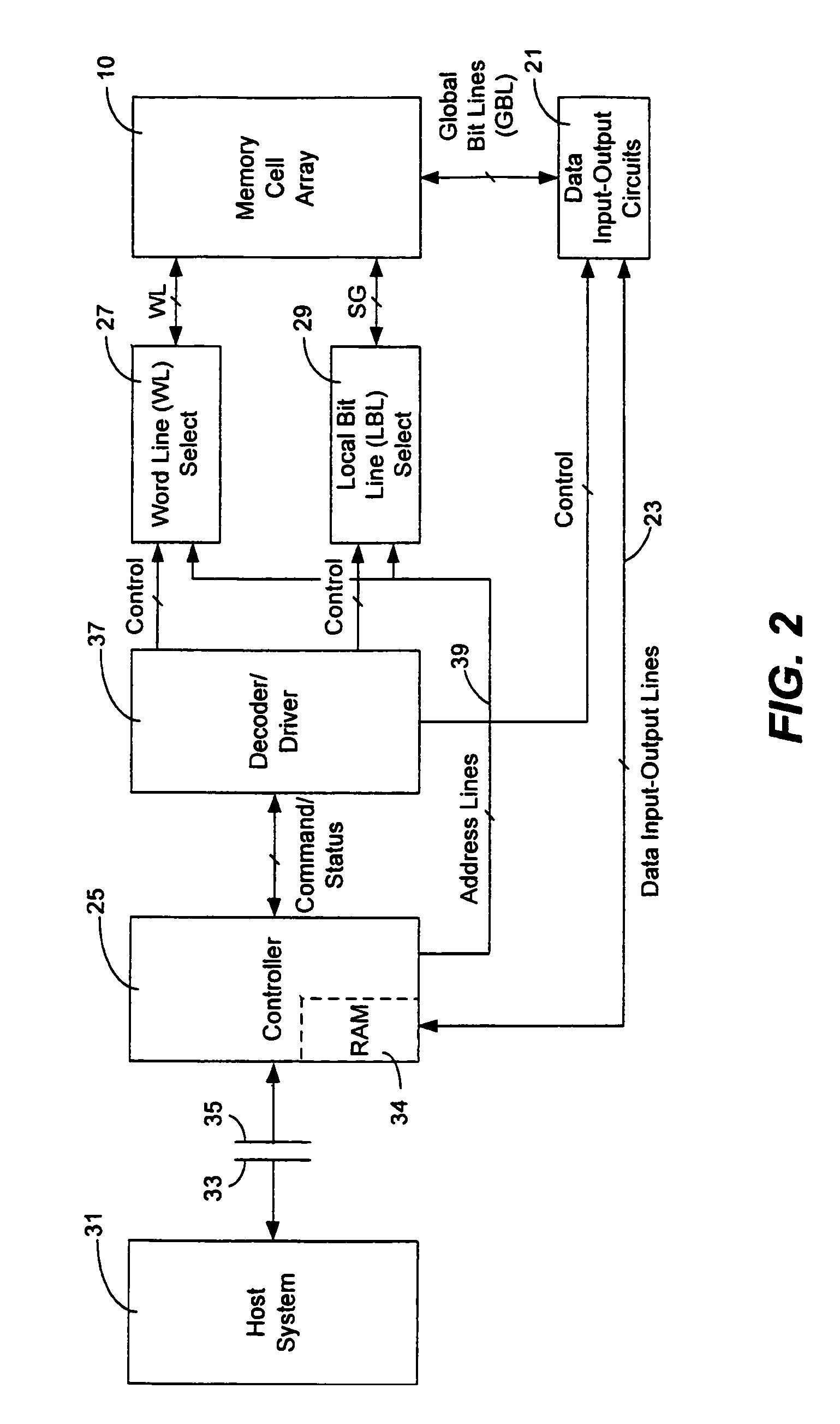
[0016]According to one aspect of the invention, a 3D memory includes memory elements arranged in a three-dimensional pattern defined by rectangular coordinates having x, y and z-directions and with a plurality of parallel planes stacked in the z-direction. The memory elements in each plane are accessed by a plurality of word lines and local bit lines in tandem with a plurality of global bit lines. The plurality of local bit lines are in the z-direction through the plurality of planes and arranged in a two dimensional rectangular array of rows in the x-direction and columns in the y-directions. The plurality of word lines in each plane are elongated in the x-direction and spaced apart in the y-direction between and separated from the plurality of local bit lines in the individual planes. A non-volatile, reprogramming memory element is located near a crossing between a word line and local bit line and accessible by the word line and bit line and wherein a group of memory elements are accessible in parallel by a common word line and a row of local bit lines. The 3D memory further includes a double-global-bit line architecture with two global bit lines respectively serving even and odd local bit lines in a column thereof in the y-direction. This architecture allows one global bit line to be used by a sense amplifier to access a selected local bit line and the other global bit line to be used to access an unselected local bit lines adjacent the selected local bit line in the y-direction. In this way the adjacent, unselected local lines can be set to exactly a reference voltage same as that of the selected local bit line in order to eliminate leakage currents between adjacent bit lines.Single-Sided Word Line Architecture
[0018]The single-sided word line architecture has the advantage of decoupling local bit-line to local bit line coupling across the plurality of word lines in the y-direction. Thus, leakage currents between local bit lines are eliminated.

