Capacitor with hafnium, lanthanum and oxygen mixed dielectric and method for fabricating the same

a dielectric and hafnium-lanthanum technology, applied in the direction of fixed capacitor details, semiconductor/solid-state device details, fixed capacitors, etc., can solve the problem of no capacitor showing a limitation of securing the capacitance of greater than 256 m, high current leakage, and the limitation of securing the capacitance of the capacitor, so as to reduce the level of leakage current incidence and reduce the equivalent oxide thickness

Inactive Publication Date: 2008-01-22
SK HYNIX INC
View PDF6 Cites 2 Cited by
  • Summary
  • Abstract
  • Description
  • Claims
  • Application Information

AI Technical Summary

Benefits of technology

[0012]It is, therefore, an object of the present invention to provide a capacitor with a dielectric layer having a low equivalent oxide thickness compared to the HfO2 layer and capable of decreasing a level of a leakage current incidence and a method for fabricating the same.

Problems solved by technology

Furthermore, the NO capacitor shows a limitation of securing the capacitance of greater than 256 M required for a next generation DRAM product.
However, Ta2O5 has a smaller band gap than SiO2 or Si3N4, thereby having a high current leakage.
However, there is a limitation of securing the capacitance of the capacitor since the Al2O3 layer does not have the large dielectric constant (ε).
However, the HfO2 layer has a problem of increasing the leakage current during a subsequent thermal process due to a structural weakness of the layer itself.
Furthermore, if the thermal process is proceeded at a temperature of higher than 700° C., the leakage current is abruptly increased and all of memory information is lost.
Also, there is a problem of a decrease in tolerance of the capacitor, and thus, the HfO2 layer is very weak to a repeated electric shock due to a low breakdown voltage of the HfO2 layer itself.
In addition, if the thermal process proceeds to the HfO2 layer at a high temperature in an atmosphere of oxygen, the HfO2 layer cannot have a limit thickness with respect to tolerance to oxidation and a silicon oxide layer (SiO2) is abruptly increased at an interface between a bottom electrode and the HfO2 layer.
Accordingly, it is difficult to make a thin HfO2 layer.

Method used


Image

  • Capacitor with hafnium, lanthanum and oxygen mixed dielectric and method for fabricating the same
  • Capacitor with hafnium, lanthanum and oxygen mixed dielectric and method for fabricating the same
  • Capacitor with hafnium, lanthanum and oxygen mixed dielectric and method for fabricating the same

Examples


Embodiment Construction

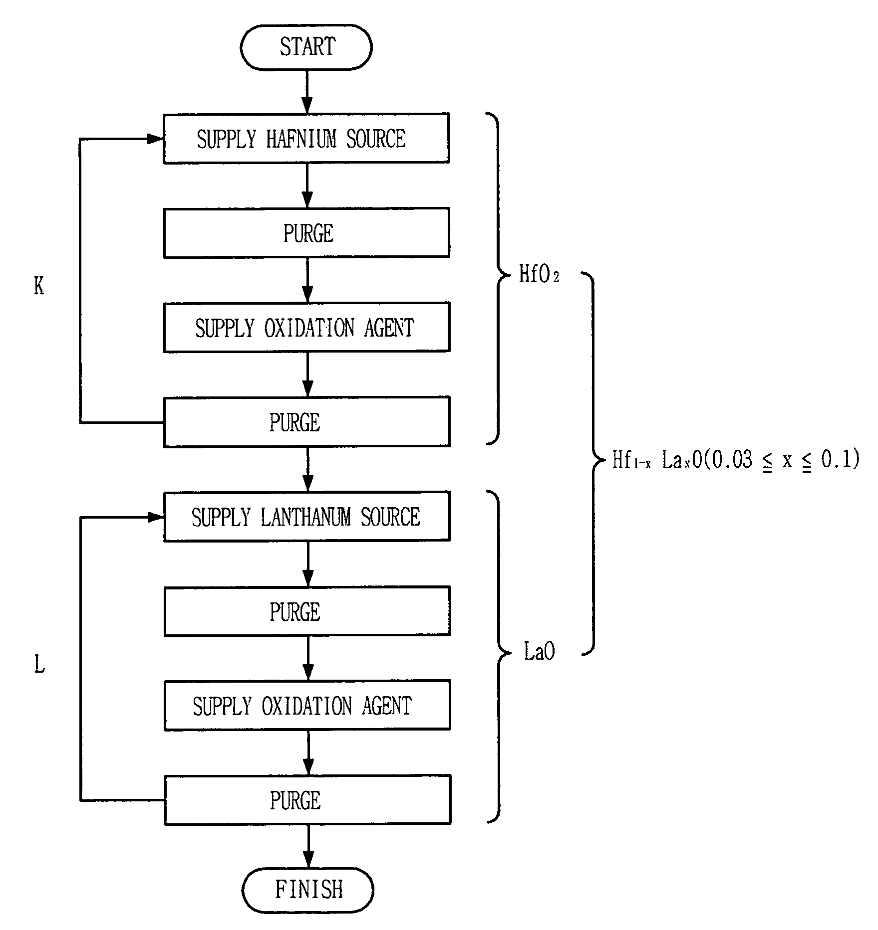
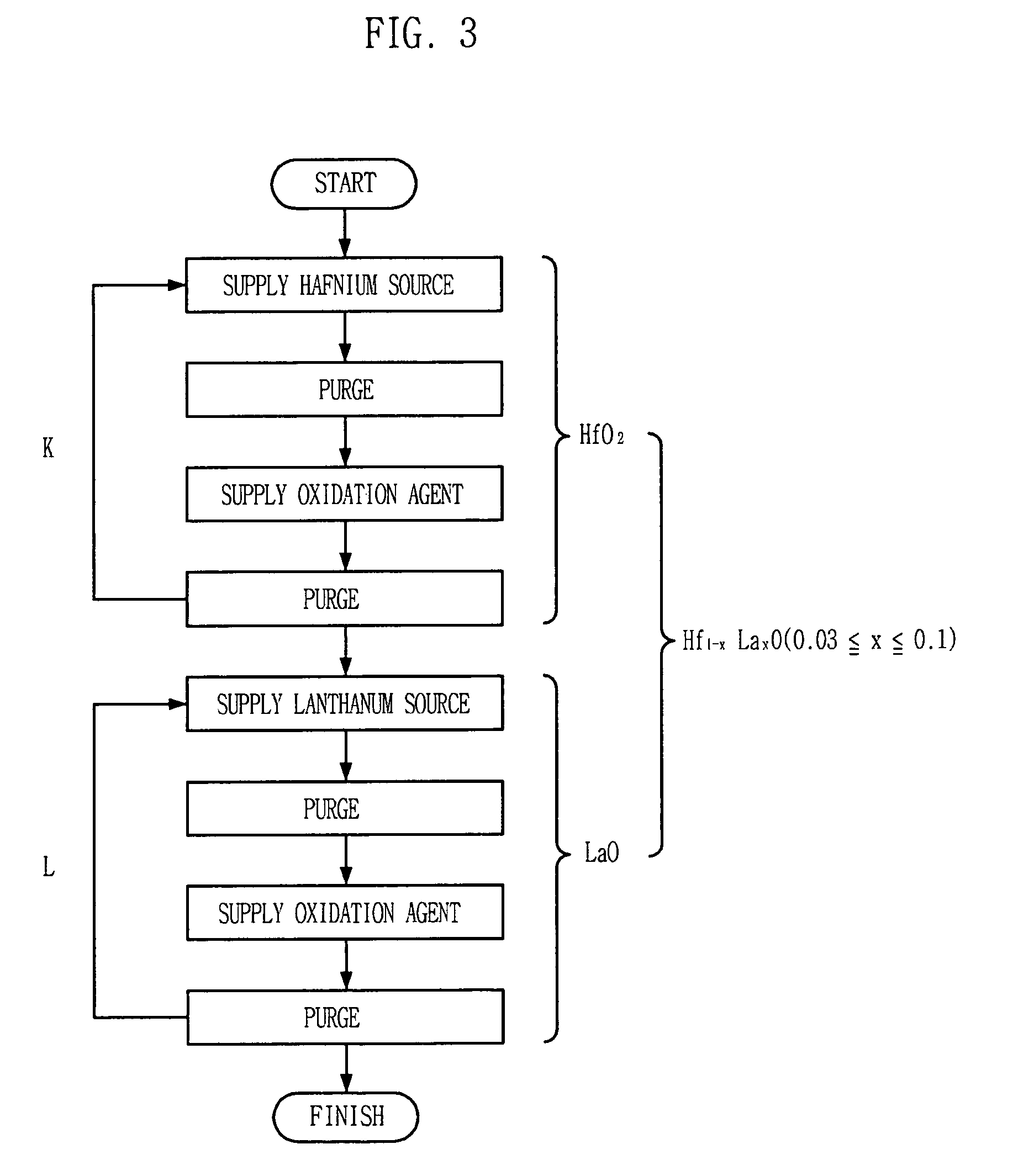
[0023]Hereinafter, detailed descriptions on preferred embodiments of the present invention will be provided with reference to the accompanying drawings.

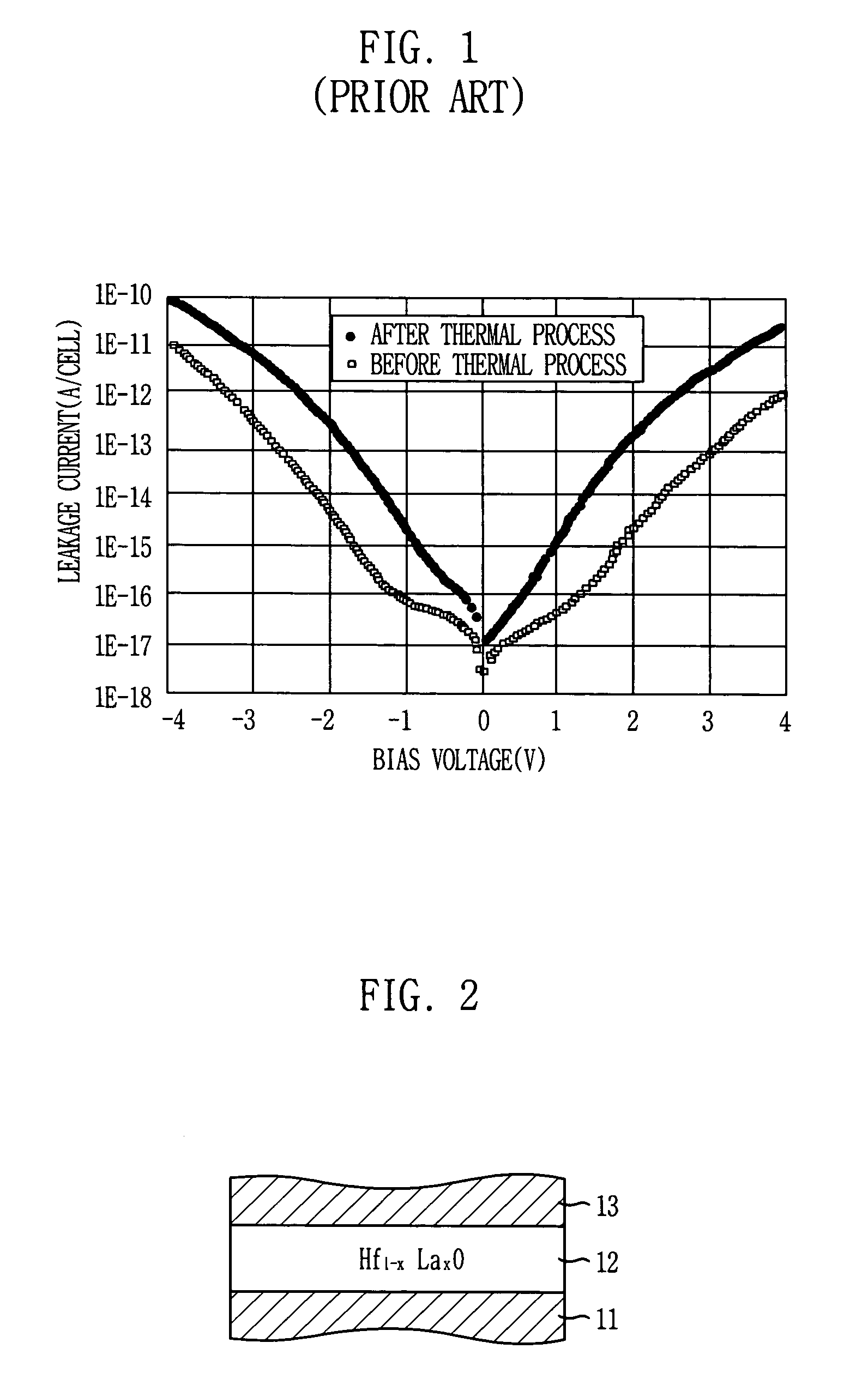
[0024]FIG. 2 is a cross-sectional view illustrating a structure of a capacitor in accordance with a preferred embodiment of the present invention.

[0025]As shown, the capacitor is formed by sequentially stacking a bottom electrode 21, a molecular structure of hafnium, lanthanum and oxygen 22 and an upper electrode 23. Hereinafter, the hafnium, lanthanum and oxygen have a Hf1-xLaxO layer, in which x represents molecular composition ratio.

[0026]More specifically, the bottom electrode 21 and the upper electrode 23 are made of a metal conductive material selected from a group consisting of phosphorus (P) or arsenic (As) doped polysilicon, titanium nitride (TiN), ruthenium (Ru), ruthenium oxide (RuO2), platinum (Pt), iridium (Ir) and iridium oxide (IrO2). For instance, the bottom electrode 21 and the upper electrode 23 are made of polysili...


PUM

PropertyMeasurementUnit
concentrationaaaaaaaaaa
temperatureaaaaaaaaaa

Abstract

Disclosed is a capacitor with a dielectric layer having a low equivalent oxide thickness compared to a HfO2 layer and capable of decreasing a level of a leakage current incidence and a method for fabricating the same. Particularly, the capacitor includes: a bottom electrode; a Hf1-xLaxO layer on the bottom electrode; and a top electrode on the Hf1-xLaxO layer, wherein x is an integer. The method includes the steps of: forming at least one bottom electrode being made of polysilicon doped with impurities; nitriding a surface of the bottom electrode; depositing the amorphous Hf1-xLaxO layer on the nitrided surface of the bottom electrode; performing a thermal process for crystallizing the amorphous Hf1-xLaxO layer and removing impurities existed within the Hf1-xLaxO layer; nitriding a surface of the crystallized Hf1-xLaxO layer; and forming the top electrode being made of polysilicon doped with impurities on the nitrided surface of the crystallized Hf1-xLaxO layer.

Description

FIELD OF THE INVENTION[0001]The present invention relates to a method for fabricating a semiconductor device; and more particularly to a capacitor and a method for fabricating the same.DESCRIPTION OF RELATED ARTS[0002]Recently, an accelerated integration level of semiconductor memory devices has led to a sharp decrease in a unit cell area. Also, an operation voltage has been decreased to a low level. However, despite of the decreased cell area, a minimum capacitance required for operating a memory device is greater than 25 fF / cell in order to prevent incidences of soft error and shortened refresh time.[0003]In general, even though a nitride / oxide (NO) capacitor of a dynamic random access memory (DRAM) using Si3N4 as a dielectric layer uses a three dimensional storage node having a large electrode surface of a hemisphere shape, a height of the storage node should be continuously increased in order to secure the large capacitance.[0004]Furthermore, the NO capacitor shows a limitation ...

Claims


Application Information

Patent Timeline
Patent Type & Authority Patents(United States)
IPC IPC(8): H01L21/31H01L21/469C23C16/40H01L27/04C23C16/455C23C16/52H01G4/08H01G4/10H01L21/314H01L21/316
CPCC23C16/40C23C16/45529C23C16/45531C23C16/52H01G4/085H01G4/10H01L21/3142H01L21/31645H01L21/31637H01L21/02192H01L21/02181H01L21/02271H01L21/0228H01L27/04
Inventor LEE, KEE-JEUNG
Owner SK HYNIX INC
Why Eureka
Try Eureka