A power device with improved diffusion region morphology and its manufacturing method

A technology of diffusion area and power device, applied in semiconductor/solid-state device manufacturing, semiconductor devices, electrical components, etc., can solve the problems of large leakage, unsatisfactory morphology of diffusion area, and many recombination centers, and achieves the reduction of leakage level and excellent performance. Thermal stability, the effect of improving the morphology

Active Publication Date: 2017-09-29
BYD SEMICON CO LTD +1
View PDF3 Cites 0 Cited by
  • Summary
  • Abstract
  • Description
  • Claims
  • Application Information

AI Technical Summary

Problems solved by technology

There is also a method to improve thermal reliability. The isolation layer between the gate region and the emitter is a composite film composed of silicon nitride and phosphorus-doped silicon nitride. Although this method can improve the thermal stability of the device, it does not Fundamentally solve the problems of unsatisfactory morphology of the diffusion area near the device surface, many recombination centers, and large leakage

Method used


Image

  • A power device with improved diffusion region morphology and its manufacturing method
  • A power device with improved diffusion region morphology and its manufacturing method
  • A power device with improved diffusion region morphology and its manufacturing method

Examples


Embodiment Construction

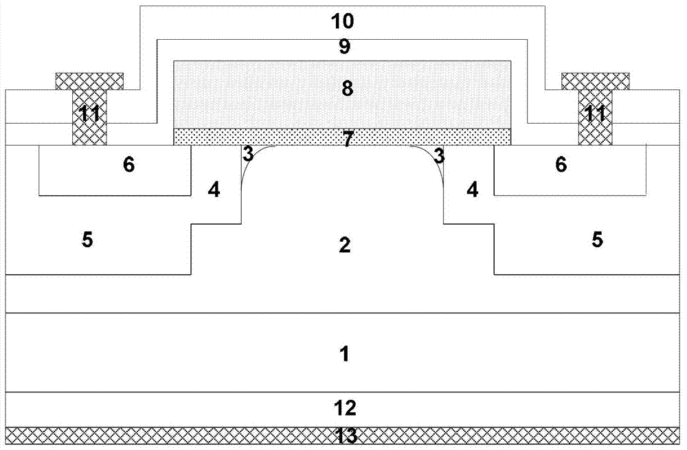
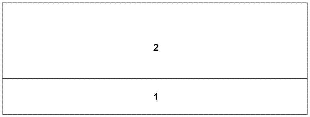
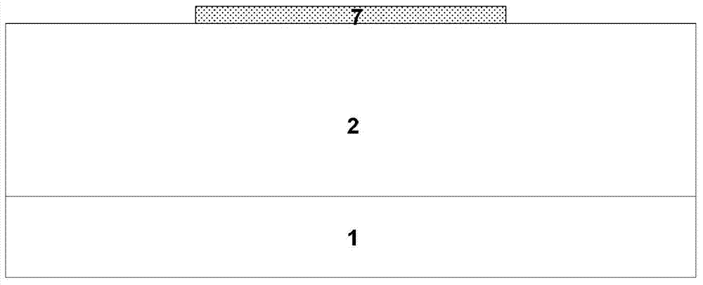
[0044] Embodiments of the present invention are described in detail below, examples of which are shown in the drawings, wherein the same or similar reference numerals designate the same or similar elements or elements having the same or similar functions throughout. The embodiments described below by referring to the figures are exemplary only for explaining the present invention and should not be construed as limiting the present invention.

[0045] In describing the present invention, it should be understood that the terms "longitudinal", "transverse", "upper", "lower", "front", "rear", "left", "right", "vertical", The orientation or positional relationship indicated by "horizontal", "top", "bottom", "inner", "outer", etc. are based on the orientation or positional relationship shown in the drawings, and are only for the convenience of describing the present invention and simplifying the description, rather than Nothing indicating or implying that a referenced device or elemen...


PUM


Abstract

The invention provides a power device for improving morphology of a diffusion region and a manufacture method thereof. The power device comprises a substrate, an epitaxial layer, a buried layer, and a source region. The buried layer between the source region and the epitaxial layer is a conducting channel region. A prediffusion region is formed in the epitaxial layer close to the conducting channel region. The power device further comprises a gate dielectric layer, a gate electrode, a dielectric layer, a front metal layer, a back diffusion region, and a back metal layer. According to the power device for improving morphology of the diffusion region, the prediffusion region enables the buried layer to be smoothly expanded towards the epitaxial layer so as to improve the morphology of the diffusion region at the edge of the channel, and optimize the electric field distribution of the power device under high temperature and high voltage. Therefore, the electric leakage level of the power device under high temperature and high voltage is reduced; and the thermal reliability of power devices such as MOSFET, IGBT, and the like can be substantially improved. The power device satisfies operating requirements in high temperature and large power environments. The manufacturing process of the power device is completely compatible with that of a conventional power device. The power device is simple in structure, convenient in manufacture, and has improved production efficiency and rate of finished products.

Description

technical field [0001] The invention belongs to the field of basic electrical components and relates to the preparation of semiconductor devices, in particular to a power device and a manufacturing method thereof which inject a layer of shallow low-concentration diffusion region to improve the morphology of the diffusion region after the gate oxide layer is completed. Background technique [0002] At present, the front-side process of power MOSFETs and IGBTs mainly includes the following steps: Taking devices prepared on N-type substrates as an example, on N-type substrates, the active region is first defined by photolithography technology, and then the gate oxide is grown. layer, and then inject N-type impurities to improve the J-FET effect of the device, then deposit polysilicon, define and etch the pattern with photolithography, and implant P-type ions in the area without polysilicon and gate oxide layer and drive them into the P-diffusion area In the P-diffusion area, th...

Claims


Application Information

Patent Timeline
Patent Type & Authority Patents(China)
IPC IPC(8): H01L29/78H01L29/10H01L21/336
CPCH01L29/1037H01L29/66333H01L29/66712H01L29/7395H01L29/7802
Inventor 乐双申徐旭东李旺勤
Owner BYD SEMICON CO LTD
Why Eureka
Try Eureka