Control of clock gating

a clock gating and control technology, applied in the direction of transmission, data conversion, sustainable buildings, etc., can solve the problems of unnecessary power consumption and achieve the effect of saving power and unnecessary power consumption

Active Publication Date: 2013-01-08
ARM LTD
View PDF7 Cites 2 Cited by
  • Summary
  • Abstract
  • Description
  • Claims
  • Application Information

AI Technical Summary

Benefits of technology

[0024]One skilled in the art will understand that adjusting the stored delay value to the ratio between the clock cycle and clock propagation delay allows refining the clock gating policy, allowing a reduction of time where the clock is asserted when not needed.
[0025]The present invention recognises that in many conventional circuits, in order for the switching from sleep to operational mode to be invisible the switching signal is asserted early so that the mode switching occurs when expected, despite any delays that may be present in the system between the signal being asserted and the clock clocking the circuit. It also recognises that for safety the wake up switching signal is asserted early enough to account for the worst case propagation delays, and therefore in situations where the propagation time is better than expected or the clocking frequency is lower, the clock reaches the module before it is required resulting in unnecessary power consumption. The present invention addresses this problem by providing a storage means for storing a delay value, such that the sending of the clock signal to the clocked circuitry can be delayed by an amount dependent upon this value. Thus, by adjusting the value stored in the data store the system can be adapted to compensate for scenarios that are better than worst case, and therefore when it estimates that the system is working under better than worst case scenario it can delay the turning on of the clock by a certain number of cycles, such that the clock signal reaches the circuitry later and thus, power is saved.
[0028]External pins can be used to input a delay value in a number of ways. For example, they can be used to set the delay value during testing of the circuit. In this way the performance of the circuit can be found and the delay value can be set accordingly. In other embodiments the external pins may be connected to external tying switches so that the delay value can be adjusted on an electronic board. This provides more flexibility allowing the value to be reset depending on circumstances.
[0030]Rather than using external pins it may be advantageous to use software that may, for example, have a program table that contains different delay values associated with different characteristics such as operating frequency, operating conditions or physical characteristics of the circuit. Thus, in response to detecting these characteristics the appropriate delay value can be sent from the software to the data store and stored there.
[0039]In some embodiments, said clock signal control circuitry further comprises a counter, said delay circuitry delaying switching of said clock signal between modes in response to a signal from said counter.
[0058]Some programs running on integrated circuits are in charge of controlling the operating frequency. This may be the case where the frequency of operation is different depending on whether the processor is powered by mains power or by a battery. The program may also be aware of the characteristics of the circuit. Thus, it may be able to set the delay values in response to its knowledge of these characteristics and / or operating conditions. In such a way the appropriate delay can be set dynamically during operation and the circuit can operate at a high power efficiency.

Problems solved by technology

It also recognises that for safety the wake up switching signal is asserted early enough to account for the worst case propagation delays, and therefore in situations where the propagation time is better than expected or the clocking frequency is lower, the clock reaches the module before it is required resulting in unnecessary power consumption.
In the case of a higher time delay or a higher operational frequency then the system is turned off later than required, again resulting in unnecessary power consumption.

Method used


Image

  • Control of clock gating
  • Control of clock gating
  • Control of clock gating

Examples


Embodiment Construction

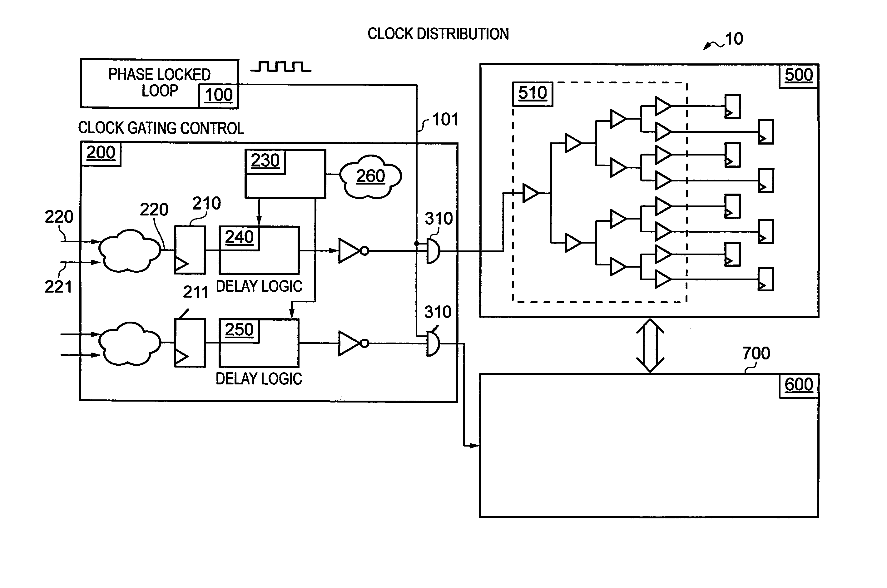
[0066]FIG. 1 shows a data processing apparatus 10 comprising a clock generation circuit 100 in the form of a phase locked loop that generates a clock signal 101, clock gating control circuitry 200 which receives this clock signal and either forwards it to processing module 500 or processing module 600 or does not forward it, but rather gates the signal.

[0067]The two modules 500 and 600 use a communication link 700 to interact one with another. Their modes of operation (either inactive, sleep mode, or active operational mode) are separately controlled and thus, their clock signals are sent or gated independently of each other by clock gating control circuit 200. Module 500 is shown as comprising a clock distribution tree 510 for distributing the clock signal to the synchronous circuitry within the module. A similar tree (not shown) is present in module 600.

[0068]The clock signal 101 is generated under the control of the Phase Locked Loop (PLL) 100. One skilled in the art will know th...


PUM


Abstract

Clock signal control circuitry is disclosed along with a method for switching a clock between modes and a computer program product. The clock signal control circuitry is for receiving a clock signal from a clock signal generator and for outputting said clock signal to synchronous circuitry that is to be clocked by said clock signal. It comprises: an input for receiving mode switching signals indicating said synchronous circuitry is to switch between modes, said mode switching signals comprising a clock gating request signal indicating said synchronous circuitry is to enter a sleep mode during which said circuitry is not clocked and a wake up request signal indicating said synchronous circuitry is to enter an operational mode during which said circuitry is clocked; and is responsive to said clock gating request signal to gate said clock signal such that no clock signal is output to said synchronous circuitry and being responsive to said wake up request signal to output said clock signal to said synchronous circuitry. The clock signal control circuitry further comprises: a data store for storing a delay value; and delay circuitry for delaying switching of said clock signal between modes in response to at least one of said mode switching signals, said delay circuitry delaying said switching by an amount dependent upon said stored delay value.

Description

[0001]This application claims priority to GB Application No. 0823249.8, filed Dec. 19, 2008, the entire contents of which are hereby incorporated by reference.BACKGROUND OF THE INVENTION[0002]1. Field of the Invention[0003]The present invention relates to the field of clock gating control within synchronous circuitry.[0004]2. Description of the Prior Art[0005]Synchronous circuitry that is clocked by a clock signal may have that clock signal turned off or gated during non-operational periods or sleep modes to conserve power. Such power saving may involve gating the clock signal sent to a complete system when the system is not in use. Alternatively, the clock for just a part of the system, which we will refer to as a module, can be gated when that module is not operational. On an even finer basis, the clock can be gated for just a single element, for example a Flip Flop.[0006]When gating on a module basis, the clock is usually gated early in the clock distribution tree of the module. ...

Claims


Application Information

Patent Timeline
Patent Type & Authority Patents(United States)
IPC IPC(8): G06F11/00
CPCG06F1/10G06F1/3203G06F1/3237Y02B60/1221Y02D10/00G06F11/3419
Inventor TEYSSIER, REMIBEGON, FLORENTJAUBERT, JOCELYN FRANCOIS ORIONAIRAUD, CEDRIC DENIS ROBERT
Owner ARM LTD
Why Eureka
Try Eureka