Optical module package unit

a technology of optical modules and package units, applied in wave based measurement systems, instruments, reradiation, etc., can solve the problems of low luminous efficiency of light-emitting chips, low packaging cost of proximity optical sensor modules, and instability of readings of handheld electronic devices, so as to improve product competitiveness and reduce packaging costs

Active Publication Date: 2013-01-29
LINGSEN PRECISION INDS
View PDF65 Cites 54 Cited by
  • Summary
  • Abstract
  • Description
  • Claims
  • Application Information

AI Technical Summary

Benefits of technology

[0007]The present invention has been accomplished under the circumstances in view. It is the main object of the present invention to provide an optical module package unit, which effectively lowers the packaging cost, enhancing product competitiveness.

Problems solved by technology

As the light-emitting chip and the light sensor chip are separately packaged, the packaging cost of the proximity optical sensor module remains high.
Further, after packaging of the aforesaid conventional proximity optical sensor module, the light-emitting chip has a low luminous efficiency, and the mating light sensor chip may receive a poor light signal, resulting reading instability of the handheld electronic device.

Method used


Image

  • Optical module package unit
  • Optical module package unit
  • Optical module package unit

Examples


Embodiment Construction

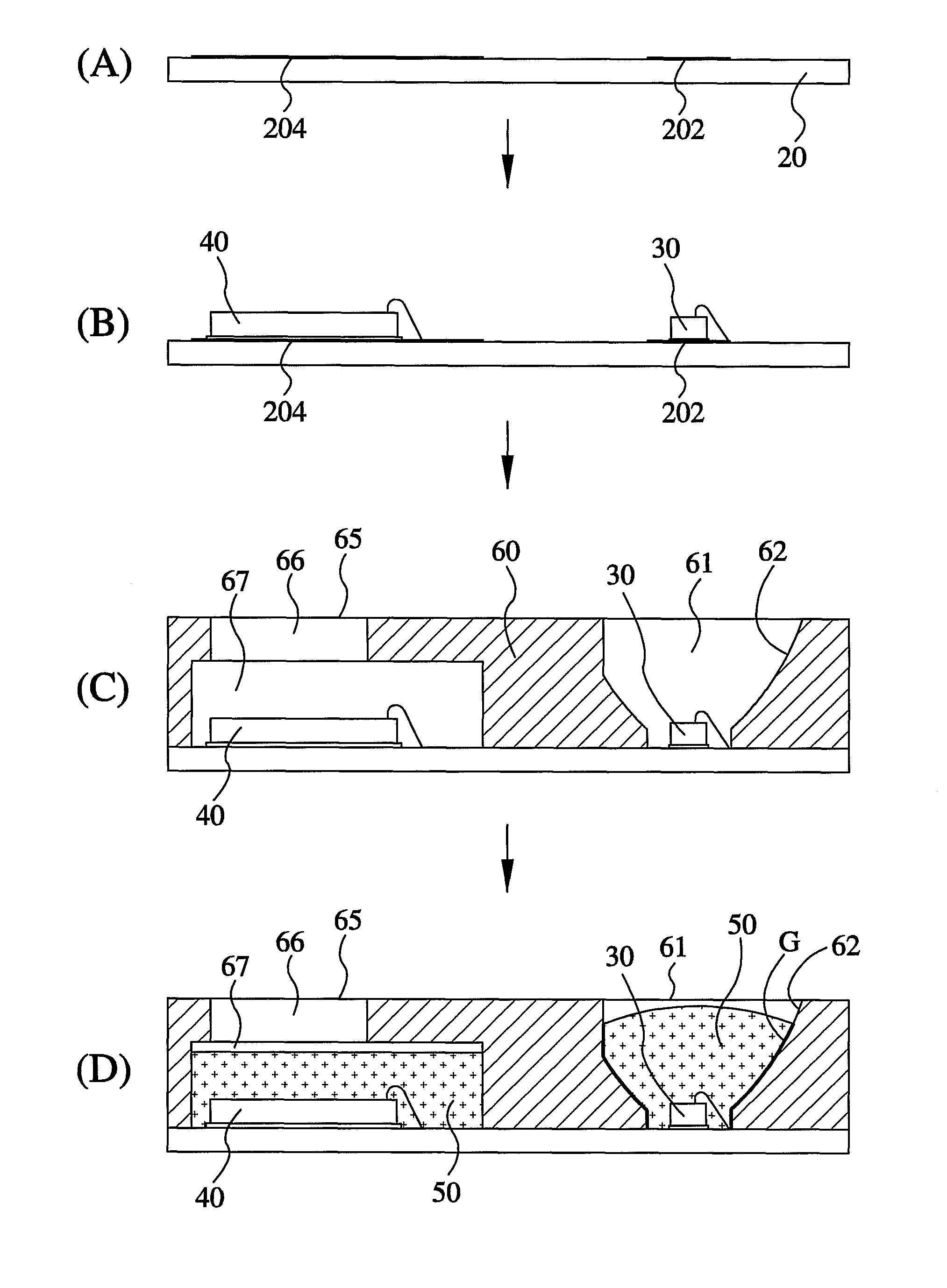
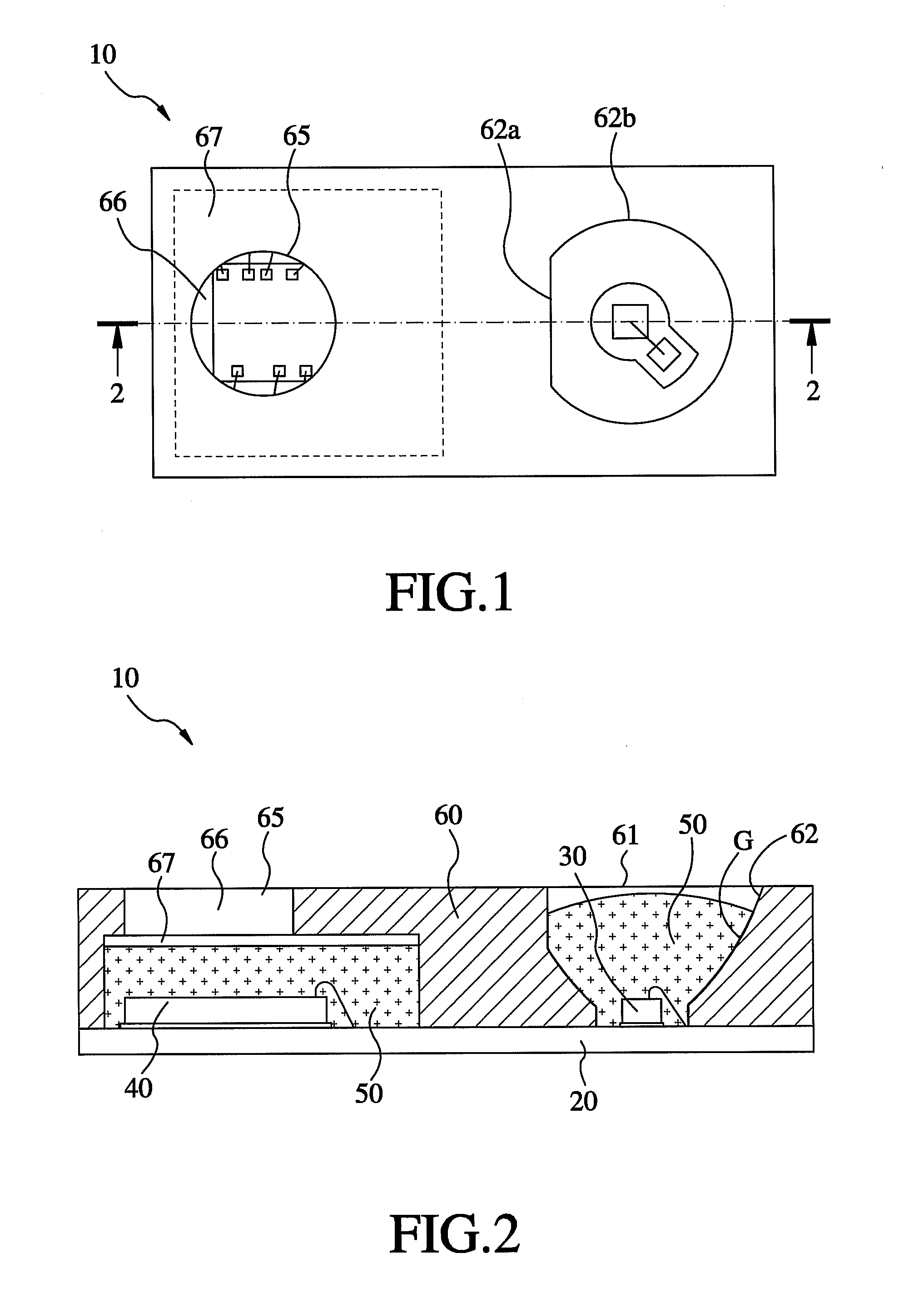
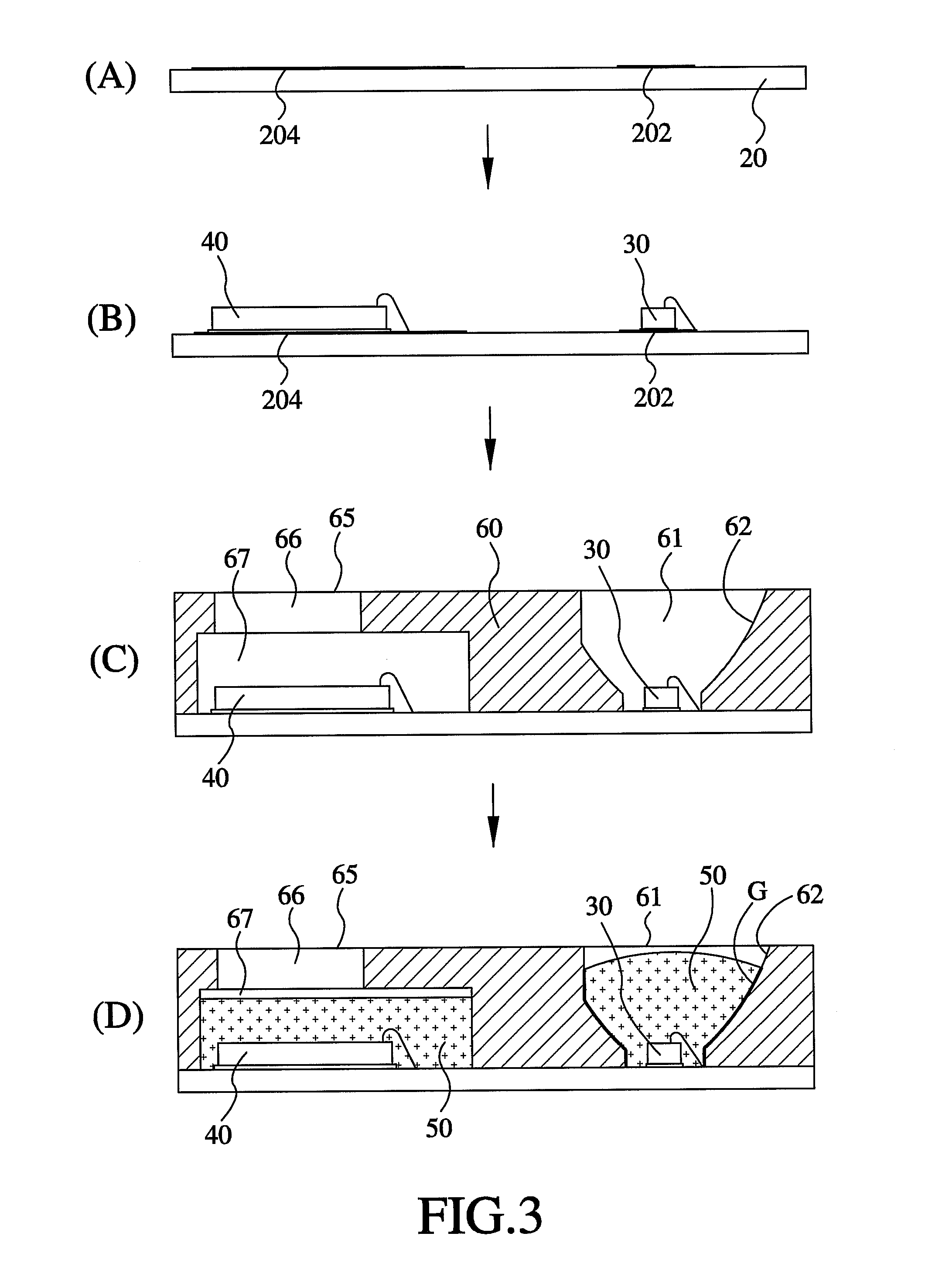
[0016]Referring to FIGS. 1˜3, an optical package unit 10 is cut from an array package. The optical package unit 10 comprises a substrate 20, a light-emitting chip 30, a light sensor chip 40, two packaging adhesive members 50 and a lid 60.

[0017]The substrate 20 according to this embodiment is not a ceramic substrate. It can be prepared from organic BT (bismaleimide triazine) resin or FR4 glass epoxy for the advantages of low manufacturing cost and high mechanical values and electrical insulating qualities. The substrate 20 defines a light-emitting zone 202 and a light-sensing zone 204.

[0018]The light-emitting chip 30 and the light sensor chip 40 are respectively installed in the light-emitting zone 202 and light-sensing zone 204 of the substrate 20 by means of die-attaching and wire-bonding processes. The light-emitting chip 30 is adapted for emitting light. The light sensor chip 40 is adapted for sensing the light source emitted by the light-emitting chip 30.

[0019]The lid 60 is a th...


PUM


Abstract

An optical module package unit includes a light-emitting chip and a light sensor chip respectively installed in a light-emitting zone and a light-sensing zone on a substrate, a lid of plastic shell integrally formed on the substrate and defining therein a first cavity and a second cavity around the light-emitting chip and the light sensor chip respectively, and two packaging adhesive structures respectively molded in the first cavity and the second cavity to encapsulate the light-emitting chip and the light sensor chip respectively. As the light-emitting chip and the light sensor chip are integrally packaged on the substrate, the packaging cost of the optical module is significantly lowered.

Description

BACKGROUND OF THE INVENTION[0001]1. Field of the Invention[0002]The present invention relates to optical module packaging technology and more particularly, to an optical module package unit, which effectively lowers the optical module packaging cost.[0003]2. Description of the Related Art[0004]To avoid accidental touching of the touch screen or to save power consumption, a handheld electronic device (such as smart phone) is generally equipped with a proximity optical sensor module. When the handheld electronic device is in proximity to the surface of an object (for example, the face of a person), the proximity optical sensor module is induced to switch off a part of the power supply. The proximity optical sensor module uses a light-emitting chip to emit a light source, and a light sensor chip to receive the light that is emitted by the light-emitting chip and reflected by a media (for example, the face) and then to convert the light signal into an electronic signal for further proce...

Claims


Application Information

Patent Timeline
Patent Type & Authority Patents(United States)
IPC IPC(8): H01L21/00
CPCH01L25/167H01L23/3107H01L2224/48091H01L2224/73265H01L2224/48227H01L2224/32225H01L2924/00014H01L2924/00G01B11/14G01S17/08
Inventor TU, MING-TEYU, CHAO-WEI
Owner LINGSEN PRECISION INDS
Why Eureka
Try Eureka