Schottky diode with extended forward current capability

a forward current capability and diode technology, applied in the field of schottky diodes, can solve the problems of bringing some parasitic effects, undesirable parametric deficiency or destructive failure, and limited forward current ability of low leakage schottky diodes

Active Publication Date: 2013-02-05
CHENGDU MONOLITHIC POWER SYST
View PDF6 Cites 3 Cited by
  • Summary
  • Abstract
  • Description
  • Claims
  • Application Information

AI Technical Summary

Benefits of technology

[0002]In integrated circuit technology, the Schottky diode has many important advantages over the regular diode such as low forward voltage drop, being majority carrier device, fast switching and so on. Meanwhile, it is required to enhance or to improve some performances of the Schottky diode, for example, a higher forward current, a lower leakage current, a higher breakdown voltage, etc.

Problems solved by technology

However, P-type guard ring 108 also brings some parasitic effects.
For example, when a large forward current flows through Schottky diode100, a serious minority injection and a PNP transistor action may occur, and this may lead to either undesirable parametric deficiency or destructive failure.
Hence the forward current ability of low leakage Schottky diode is limited.

Method used


Image

  • Schottky diode with extended forward current capability
  • Schottky diode with extended forward current capability
  • Schottky diode with extended forward current capability

Examples


Embodiment Construction

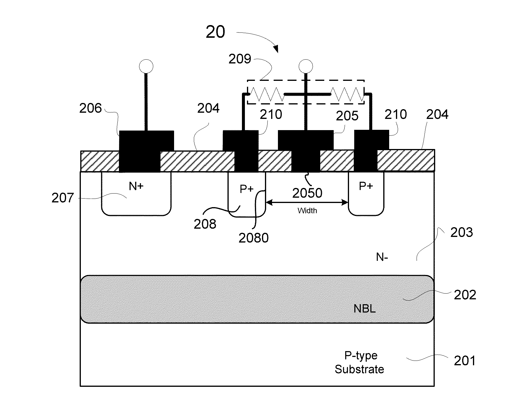
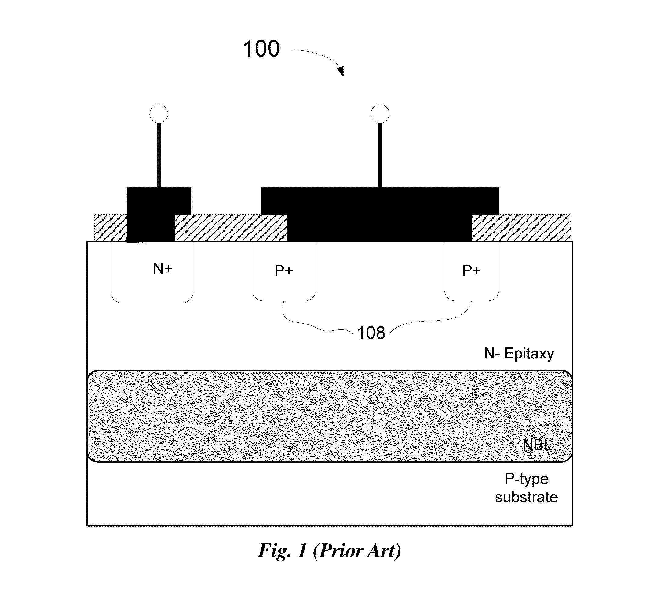
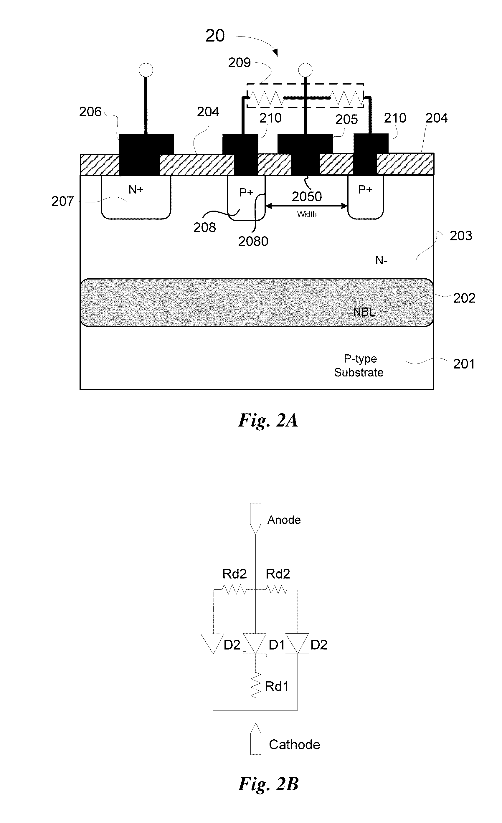
[0017]Reference will now be made in detail to the preferred embodiments of the invention, examples of which are illustrated in the accompanying drawings. While the invention will be described in conjunction with the preferred embodiments, it will be understood that they are not intended to limit the invention to these embodiments. On the contrary, the invention is intended to cover alternatives, modifications and equivalents, which may be included within the spirit and scope of the invention as defined by the appended claims. Furthermore, in the following detailed description of the present invention, numerous specific details are set forth in order to provide a thorough understanding of the present invention. However, it will be obvious to one of ordinary skill in the art that the present invention may be practiced without these specific details. In other instances, well-known methods, procedures, components, and circuits have not been described in detail so as not to unnecessarily...


PUM


Abstract

The embodiments of the present invention disclose a semiconductor device and a method for forming the semiconductor device. Wherein the semiconductor comprises: a first semiconductor layer, having a first conductivity type on a semiconductor substrate, a guard ring region, formed in the surface of the first semiconductor layer, having a second conductivity type; a Schottky diode metal contact, coupled to the first semiconductor layer, wherein the guard ring region is at periphery of the Schottky diode interface, and wherein the Schottky diode metal contact has no direct electrical connection with the guard ring region; and an electrical resistance module, coupled between the Schottky diode metal contact and the guard ring. Due to the ballasting effect from the electrical resistance module, the minority injection or the parasitic transistor action are alleviated. Thus, forward current capability is extended without introducing significant minority injection.

Description

TECHNICAL FIELD[0001]The present invention generally relates to semiconductor device, and more particularly but not exclusively relates to Schottky diode.BACKGROUND[0002]In integrated circuit technology, the Schottky diode has many important advantages over the regular diode such as low forward voltage drop, being majority carrier device, fast switching and so on. Meanwhile, it is required to enhance or to improve some performances of the Schottky diode, for example, a higher forward current, a lower leakage current, a higher breakdown voltage, etc.[0003]Sometimes improving one parameter needs to compromise another parameter. For an instance, a low leakage Schottky diode comes with a limited forward current capability. FIG. 1 schematically depicts a cross-section structure of a typical Schottky diode 100. Conventionally, a P-type guard ring structure 108 is comprised in diode 100 configured to improve at least the performances of breakdown voltage and leakage current. However, P-typ...

Claims


Application Information

Patent Timeline
Patent Type & Authority Patents(United States)
IPC IPC(8): H01L29/66H01L29/47H01L21/28
CPCH01L27/0814H01L29/872
Inventor URIENZA, JOSEPH
Owner CHENGDU MONOLITHIC POWER SYST
Why Eureka
Try Eureka