Multi-chip memory package with a small substrate

a memory package and substrate technology, applied in the field of semiconductor devices, can solve the problems of poor reliability, poor moisture resistance, and substrates with the same dimension as memory cards are vulnerable to peeling, and achieve the effect of reducing substrate cost and eliminating peeling from exposed cut sides

Active Publication Date: 2013-02-05
POWERTECH TECHNOLOGY
View PDF35 Cites 13 Cited by
  • Summary
  • Abstract
  • Description
  • Claims
  • Application Information

AI Technical Summary

Benefits of technology

[0004]The main purpose of the present invention is to provide a multi-chip memory package with a small substrate to reduce substrate cost and to eliminate peeling from exposed cut sides of a conventional substrate.

Problems solved by technology

However, the singluated cut sides of the substrate are exposed from the encapsulant which cause poor moisture resistivity and poor reliability.
Moreover, the substrate with the same dimension as the memory card is vulnerable for peeling due to stresses exerted on the peripheries of the memory card.
However, a leadframe is quite limited in circuitry layout with complicated wire bonding or long bonding wires where RDL may be needed on a chip surface leading to even higher chip fabrication cost.
Furthermore, no matter a leadframe or a substrate is implemented as a chip carrier, the cut ends of tie bars of a leadframe or the cut sides of a substrate after singulation would become electrically conductive and exposed to atmosphere leading to ESD issues during packaging processes or end-product implementation.

Method used


Image

  • Multi-chip memory package with a small substrate
  • Multi-chip memory package with a small substrate
  • Multi-chip memory package with a small substrate

Examples


Embodiment Construction

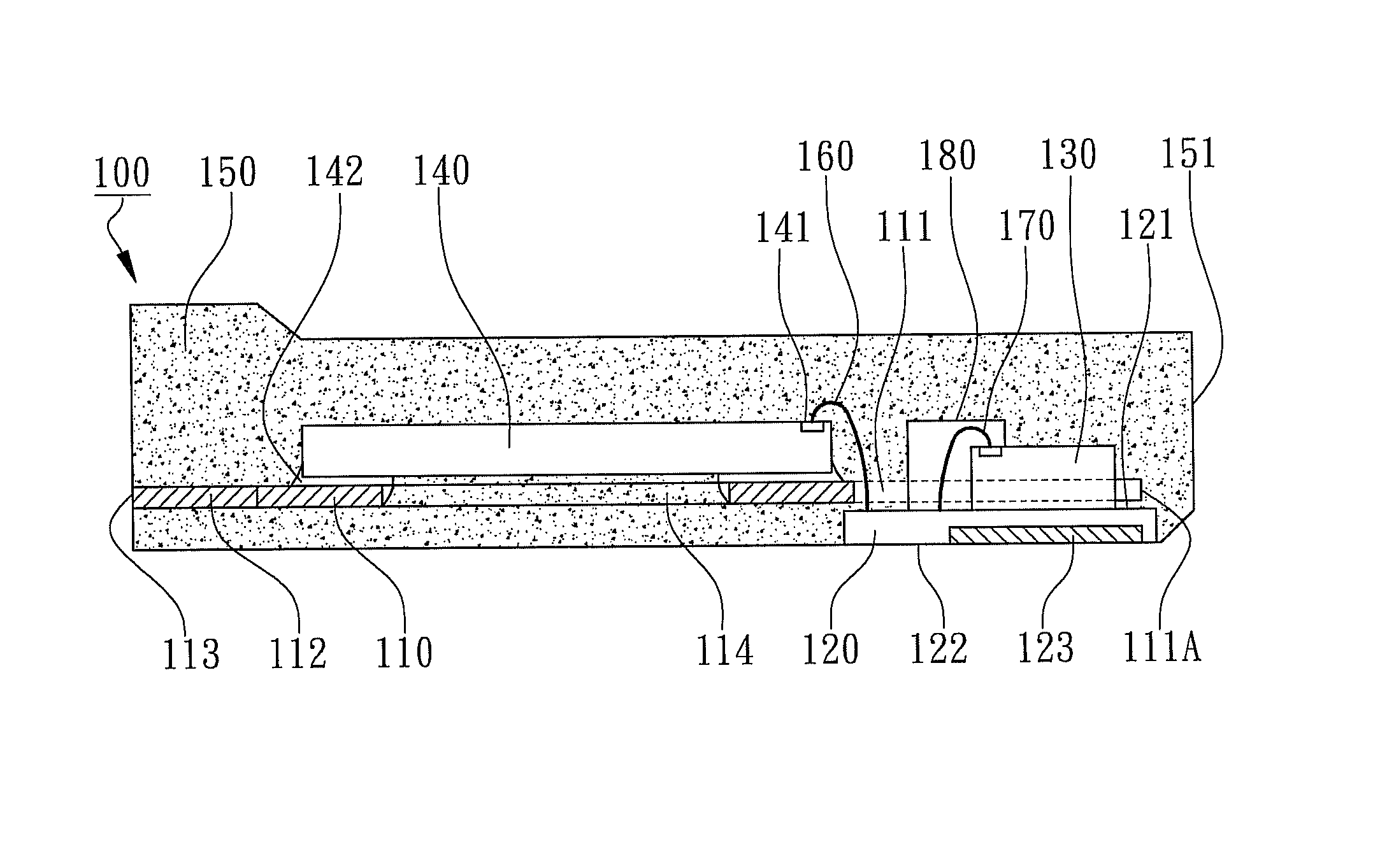
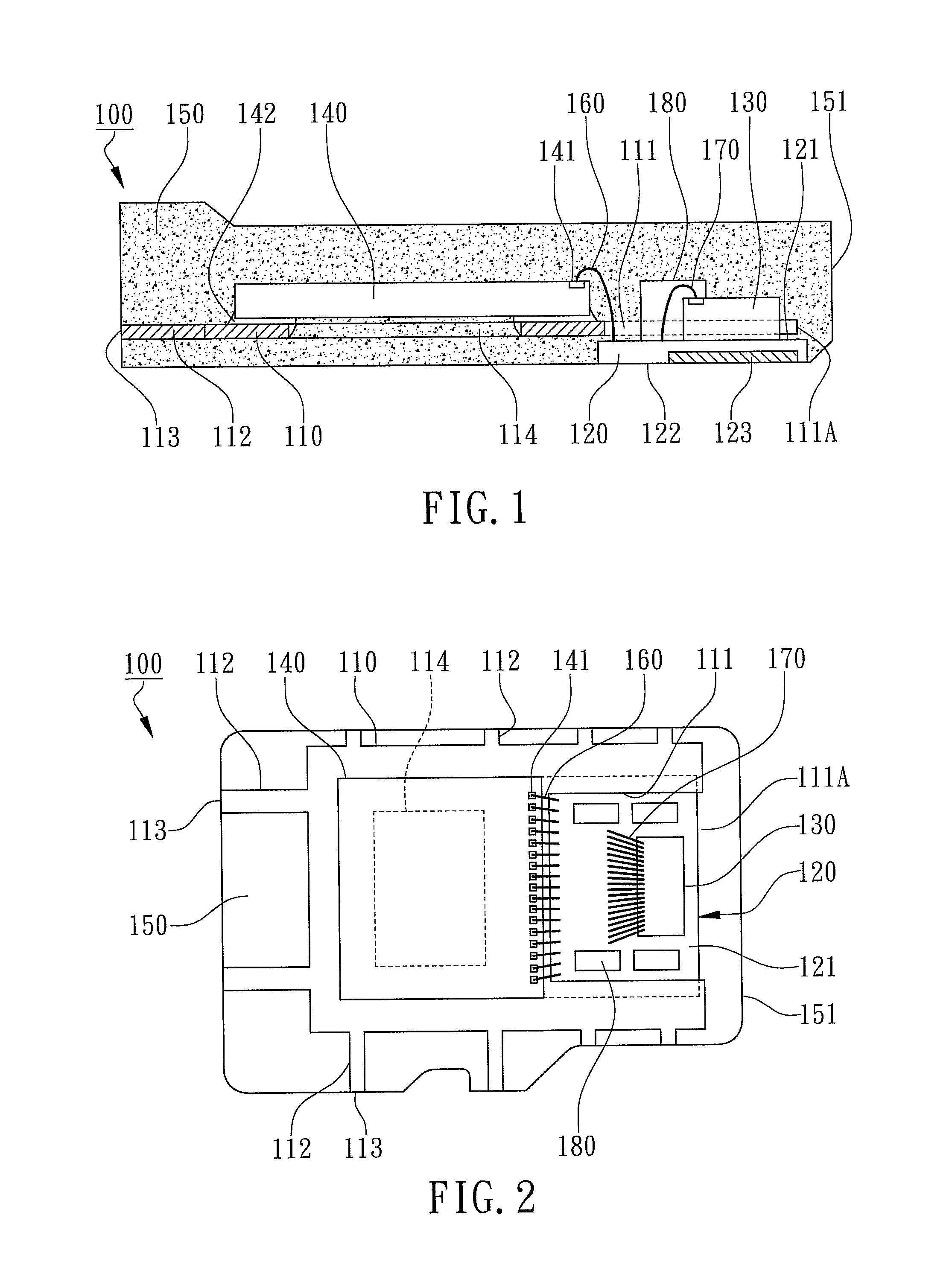
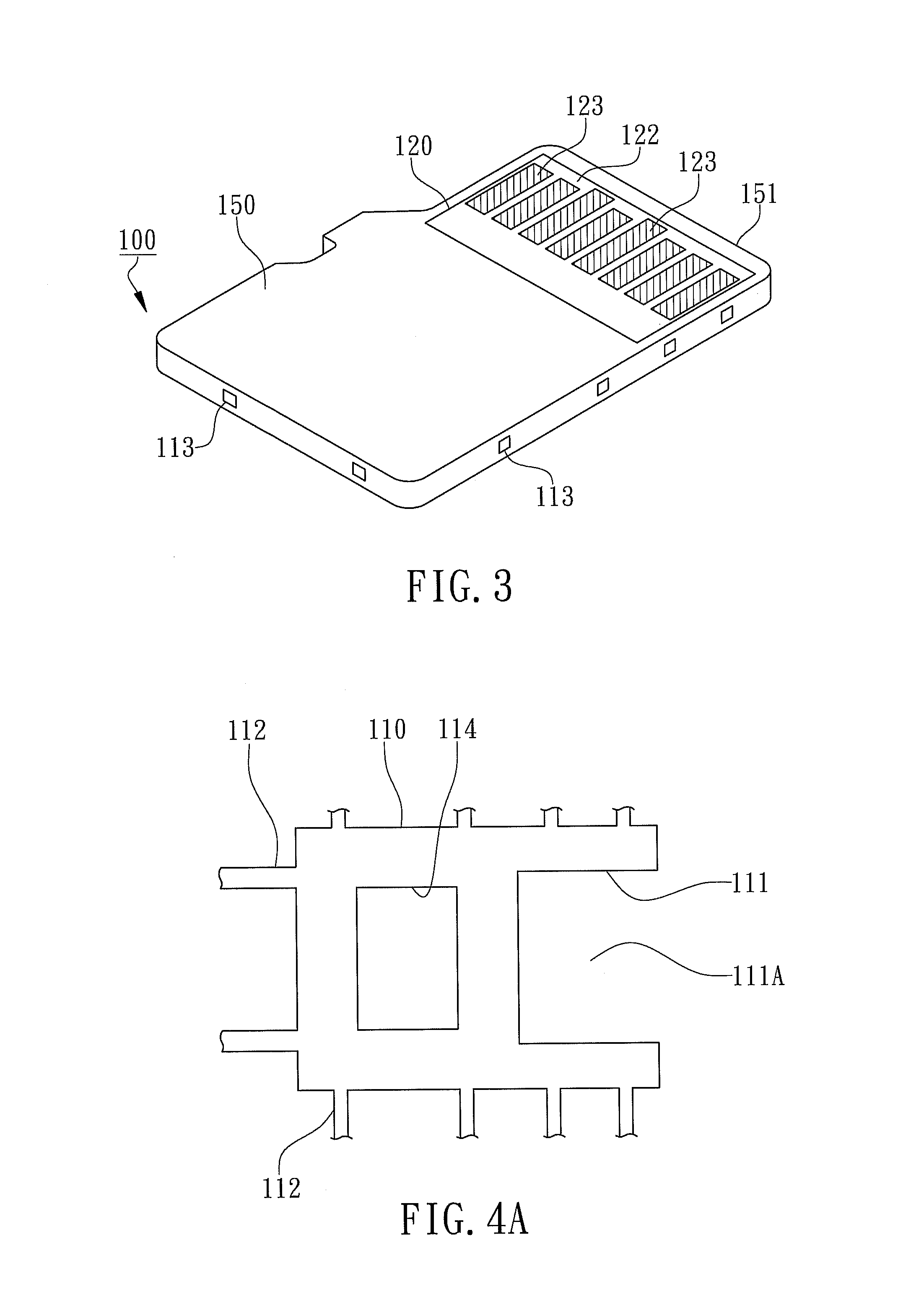
[0014]With reference to the attached drawings, the present invention is described by means of the embodiment(s) below where the attached drawings are simplified for illustration purposes only to illustrate the structures or methods of the present invention by describing the relationships between the components and assembly in the present invention. Therefore, the components shown in the figures are not expressed with the actual numbers, actual shapes, actual dimensions, nor with the actual ratio. Some of the dimensions or dimension ratios have been enlarged or simplified to provide a better illustration. The actual numbers, actual shapes, or actual dimension ratios can be selectively designed and disposed and the detail component layouts may be more complicated.

[0015]According to the preferred embodiment of the present invention, a multi-chip memory package with a small substrate is revealed where a cross-sectional view is illustrated in FIG. 1, a perspective top view seeing through...


PUM


Abstract

Disclosed is a multi-chip memory package with a small substrate by using a die pad having an opening to substitute the chip-carrying function of a conventional substrate so that substrate dimension can be reduced. A substrate is attached under the die pad. A first chip is disposed on the substrate located inside the opening. A second chip is disposed on the die pad. An encapsulant encapsulates the top surface of the die pad, the top surface of the substrate, the first chip, and the second chip. The dimension of the substrate is smaller than the dimension of the encapsulant. In a preferred embodiment, a plurality of tie bars physically connect to the peripheries of the die pad and extend to the sidewalls of the encapsulant to have a plurality of insulated cut ends exposed from the encapsulant.

Description

FIELD OF THE INVENTION[0001]The present invention relates to a semiconductor device, and more specifically to a multi-chip memory package with a small substrate.BACKGROUND OF THE INVENTION[0002]Conventionally, a substrate with the same dimension as a memory card is implemented as a chip carrier in early memory packages such as revealed in U.S. Pat. No. 7,094,633 B2. A plurality of substrates are physically interconnected in a substrate strip, then chips are disposed on the corresponding substrates followed by molding the substrate strip, and finally, the molded substrate strip is singulated into individual memory cards. However, the singluated cut sides of the substrate are exposed from the encapsulant which cause poor moisture resistivity and poor reliability. Moreover, the substrate with the same dimension as the memory card is vulnerable for peeling due to stresses exerted on the peripheries of the memory card.[0003]In order to reduce the packaging cost of memory packages, it has...

Claims


Application Information

Patent Timeline
Patent Type & Authority Patents(United States)
IPC IPC(8): H01L23/495
CPCH01L23/49531H01L23/49575H01L21/561H01L21/565H01L23/60H01L23/49541H01L23/3107H01L2224/73265H01L2224/48091H01L2924/1815H01L2924/00014
Inventor CHEN, HUI-CHANG
Owner POWERTECH TECHNOLOGY
Why Eureka
Try Eureka