
Low temperature process for TFT fabrication

a low temperature process and fabrication technology, applied in the direction of transistors, electrical equipment, semiconductor devices, etc., can solve the problems of color filter not being able to withstand temperatures exceeding 300° c. for any appreciable amount of time, the cost of manufacturing such displays in the tft-lcd market, and the inability to manufacture such displays in any manner. , to achieve the effect of eliminating peeling of the insulator, improving the fabrication process, and promoting adhesion

Active Publication Date: 2007-11-27
APPLIED MATERIALS INC
View PDF30 Cites 6 Cited by
  • Summary
  • Abstract
  • Description
  • Claims
  • Application Information

AI Technical Summary

Benefits of technology

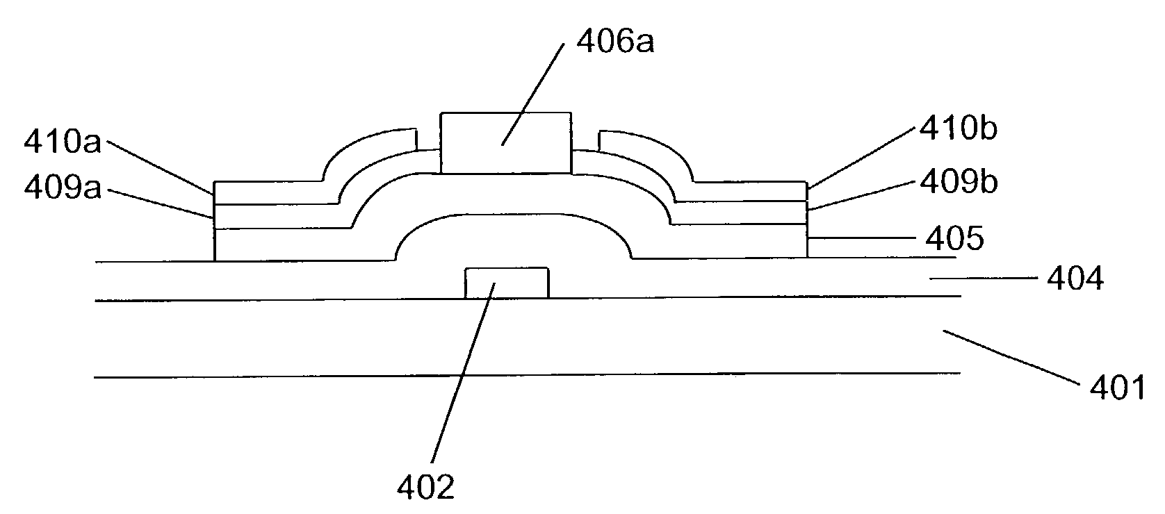
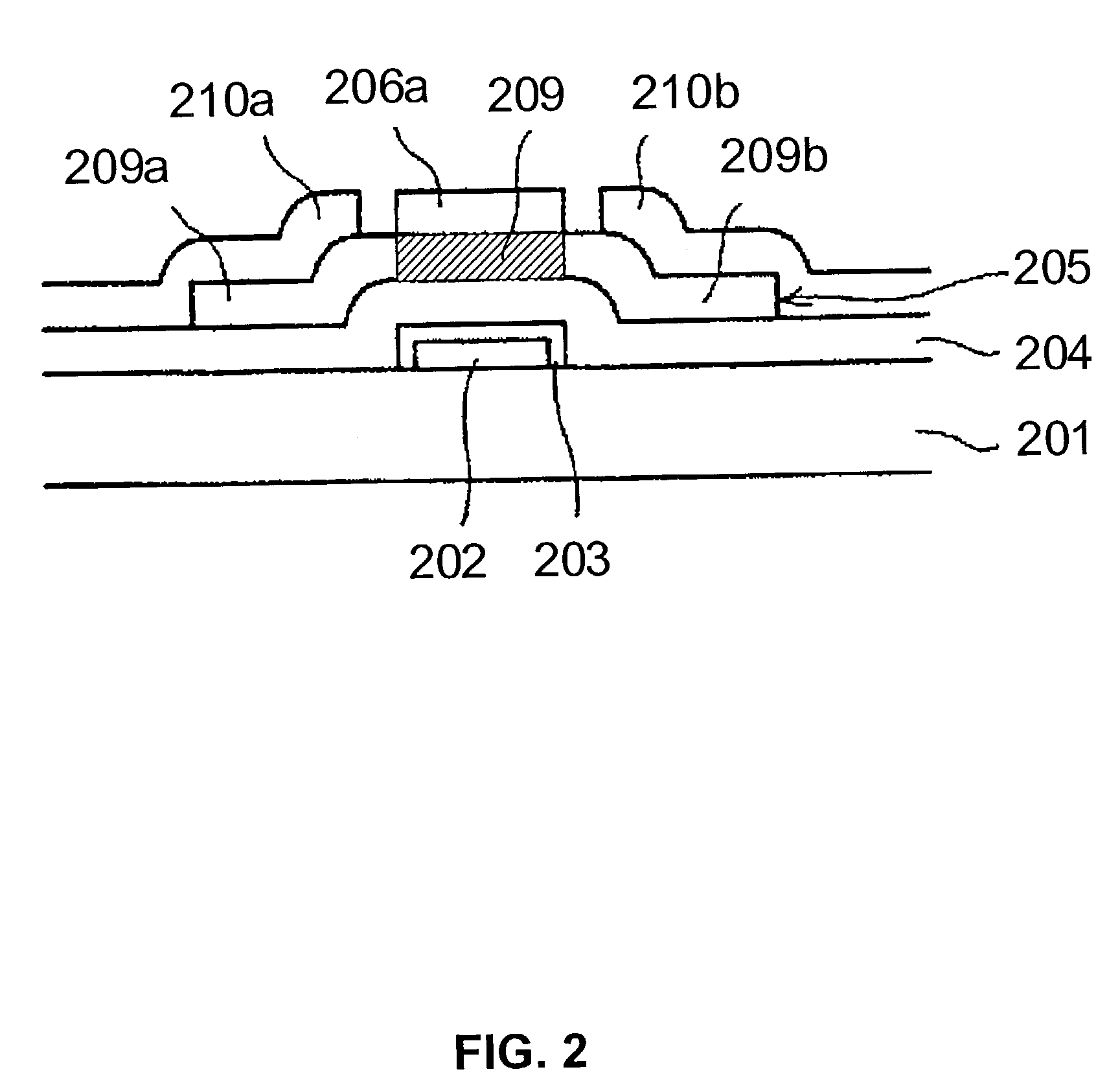
[0011]In summary, the present invention provides techniques for improving the fabrication of TFTs on low-cost, large-area substrates at low processing temperatures. The present invention provides a novel method for preparing gate metal prior to gate insulator deposition. In the novel method, gate metal is pre-treated with an H2 plasma in order to promote adhesion of the subsequently deposited gate insulator. Pretreatment of the gate metal prior to deposition of the gate insulator eliminates peeling of the insulator. Further, the present invention provides methods for improving the electrical characteristics of the gate insulating layer. It has been discovered that the layers of the gate insulator that are nearest to the active a-Si layer (FIG. 2, channel region 209) are most important in determining the electrical properties of the gate insulator layer. Accordingly, the present invention provides a dual layer approach for forming a gate insulating layer. In this dual layer approach, a high quality g-SiN film serves as an interface to the active layer while a lower stress SiN layer serves as an underlayer. The high quality layer maintains desirable TFT characteristics whereas the underlayer serves to minimize overall stress. The dual layer approach is advantageous because it takes less time to deposit the hybrid gate insulating layer, thereby improving overall throughput. Finally, the present invention provides a deposition method for incorporating phosphine into the source and drain regions of a TFT. In this deposition method, a SiH4 gas containing an impurity gas, such as PH3, is decomposed by discharge to deposit a n+ a-Si film, thereby forming the source and drain regions. It has been unexpectedly discovered that reducing the RF power relative to conventional deposition methods increases the incorporation of phosphine into the a-Si film, thus resulting in desirable resistivity.
[0014]Another aspect of the present invention provides a method of fabricating a thin-film transistor for use in a TFT-based display device. The thin-film transistor has an insulative substrate such as quartz or glass or the substrate is a color filter. In the method, a gate metal is deposited onto the substrate in order to form the gate of the thin-film transistor. Next, a first layer of a gate insulating film is deposited on the gate. Finally, a second layer of a gate insulating film is deposited onto the first layer of gate insulating film. In some embodiments, the first layer of gate insulating film has lower stress than the second layer of gate insulating film, which interfaces with the semiconductor layer. Further, the second insulating layer has better electrical properties than the first insulating layer. In some embodiments, the first layer of gate insulating film is deposited at a higher deposition rate than the first layer, thereby providing manufacturing throughput advantages.

Problems solved by technology

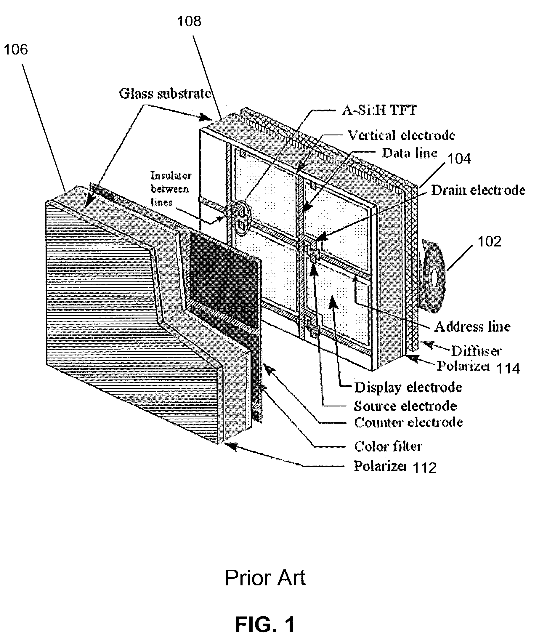
While the display-performance and screen size of TFT-LCD displays keeps improving, a critical problem in the TFT-LCD market is the cost of manufacturing such displays.
While the technique of fusing the color filter and the TFT array together is beneficial because of lower production costs, the technique imposes limitations on the manner in which the TFT array can be built.
Because of the sensitivity of organic materials to temperature, the color filter cannot withstand temperatures exceeding 300° C. for any appreciable amount of time.
In order to improve the process window for fused TFT array / color filters, Hong et al. report a thermally resistant color filter that can withstand temperatures up to 300° C. However, even with thermally stable color filters such as those reported by Hong et al., the TFT array must be built using deposition techniques that do not require susceptor temperatures exceeding 300° C. This temperature limitation is a drawback because conventional TFT manufacturing techniques rely on susceptor temperatures that are above the temperature limits for even the previously discussed high temperature color filter.
Use of susceptor temperatures substantially below 400° C. results in less desirable TFT performance characteristics.
It is likely that these less desirable performance characteristics can be correlated with film properties, such as gate insulator peeling, gate insulator layers with reduced insulating qualities, as well as reduced phosphine incorporation in the source and drain regions of the TFT.
Depending on the gate metal used in the TFT and the substrate temperature during processing, lower substrate temperatures result in poor adhesion of the gate insulating film 204 on the gate metal 202 (FIG. 2).
Subsequent peeling of the gate insulating film 204 compromises the insulating properties of the film.
Another reason low-temperature processing is not desirable is that such processing results in a decrease in substrate temperature relative to conventional deposition processes.
Low density gate insulating films have poorer insulating qualities relative to high density gate films and, as a consequence, they are undesirable.
Yet another consequence of using reduced processing temperatures, at least in the case of CVD deposition, is poor phosphine incorporation into the source and drain regions of the TFT.
However, conventional phosphorous doping is more difficult at low temperatures.
However, in many situations, even the use of higher PH3 amounts in the feed gas is insufficient to increase conductivity.

Method used


Image

  • Low temperature process for TFT fabrication
  • Low temperature process for TFT fabrication
  • Low temperature process for TFT fabrication

Examples


example 1

[0058]Processing was performed at a substrate temperature of 250° C. and an RF power of 400 watts. Silane gas flow into the PECVD chamber was 400 standard cubic centimeters per minute (sccm). PH3 was 0.5% balanced in a carrier gas. The gas flow of this PH3 mixture into the PECVD chamber was 1000 sccm. Hydrogen gas flow into the PECVD chamber was 500 sccm. The reaction resulted in the formation of an n+ doped amorphous silicon film at a deposition rate of 830 Angstroms / minute. The resistance of the resulting n+ doped amorphous silicon film was 140 ohm cm.

example 2

[0059]Processing was performed at a substrate temperature of 250° C. and an RF power of 150 watts. The gas flow of silane into the PECVD chamber was 240 standard cubic centimeters per minute (sccm). PH3 was 0.5% balanced in a carrier gas. The gas flow of this PH3 mixture into the PECVD chamber was 600 sccm. The gas flow of hydrogen into the PECVD chamber was 600 sccm. The reaction resulted in the formation of the n+ doped amorphous silicon film at a deposition rate of 570 Angstroms / minute. The resistance of the resulting n+ doped amorphous silicon film was 120 ohm cm.

example 3

[0060]Processing was performed at a substrate temperature of 150° C. and an RF power of 100 watts. The gas flow of silane into the PECVD chamber was 200 standard cubic centimeters per minute (sccm). PH3 was 0.5% balanced in a carrier gas. The gas flow of this PH3 mixture into the PECVD chamber was 400 sccm. The gas flow of hydrogen into the PECVD chamber was 800 sccm. The reaction resulted in the formation of the n+ doped amorphous silicon film at a deposition rate of 120 Angstroms / minute. The resistance of the resulting n+ doped amorphous silicon film was 220 ohm cm.


PUM


Abstract

Method of fabricating a thin-film transistor (TFT) in which a gate metal is deposited onto a substrate in order to form the gate of the thin-film transistor. The substrate may be an insulative substrate or a color filter. In a first method, the gate metal is subjected to an H2 plasma. After subjecting the gate metal to an H2 plasma, the gate insulating film is deposited onto the gate. In a second method, first and second layers of gate insulating film are respectively deposited on the gate at a first and second deposition rates. One layer is deposited under H2 or argon dilution conditions and has improved insulating conditions while the other layer serves to lower the overall compressive stress of the dual layer gate insulator. In a third method, an n+ silicon film is formed on a substrate by maintaining a flow of silane, phosphine and hydrogen gas into a processing chamber at substrate temperatures of about 300° C. or less.

Description

[0001]The present invention relates to improved methods for fabricating thin film transistors (TFTs) that use substrates such as glass, quartz, or plastic. Such TFTs are used in a number of devices, such as liquid-crystal displays. The invention also relates to TFTs that are fabricated in accordance with the improved methods.BACKGROUND OF THE INVENTION[0002]Ever since the first appearance of amorphous silicon (a-Si) thin-film transistors (TFT)-liquid crystal displays (LCDs) in notebook personal computers more than ten years ago, the number of applications for (a-Si) TFT-LCD has expanded. Fueling this expansion is the increase in screen area and the resolution of (a-Si) TFT-LCD-based display devices. Presently, (a-Si) TFT-LCD-based display devices are found in notebook PCs, modern desktop monitors, televisions, and advanced game equipment. Although the major application of the TFT technology is currently in LCDs, there are many other microelectronic products that could benefit from (...

Claims


Application Information

Patent Timeline
Patent Type & Authority Patents(United States)
IPC IPC(8): H01L21/20H01L21/336H01L21/84H01L29/49H01L29/786
CPCH01L29/4908H01L29/78678H01L29/78669H01L29/66765
Inventor HSIAO, MARKYIM, DONG-KILTAKEHARA, TAKAKOSHANG, QUANYUANHARSHBARGER, WILLIAM R.KIM, WOONG-KWONYUN, DUK-CHULCHANG, YOUN-GYUNG
Owner APPLIED MATERIALS INC
Learn More