Method and structure for eliminating edge peeling in thin-film photovoltaic absorber materials

a photovoltaic absorber and thin film technology, applied in the field of photovoltaic device manufacturing techniques, can solve the problems of film peeling and poor coverage, and achieve the effect of enhancing photovoltaic efficiency and avoiding thin film peeling

Inactive Publication Date: 2013-11-21
CM MFG
View PDF9 Cites 6 Cited by
  • Summary
  • Abstract
  • Description
  • Claims
  • Application Information

AI Technical Summary

Benefits of technology

[0005]The present invention relates generally to techniques for the manufacture of photovoltaic devices. More particularly, the present invention provides a method and structure for eliminating peeling of a photovoltaic absorber film from the lower conductive material. Merely by way of examples, the method includes patterning a conductive film to form a trench structure to isolate peripheral edge region for ensuring the thin-film photovoltaic absorber on main surface region substantially free from peeling off caused by impurity from the edge region, but it would be recognized that the invention may have other applications.
[0006]In a specific embodiment, the present invention provides a method for manufacturing a thin-film photovoltaic device free of film peeling problem. The method includes providing a soda lime glass substrate containing sodium species and having a surface region and a peripheral edge region surround the surface region. The method further includes forming a barrier material overlying the surface region and partially overlying the peripheral edge region. Additionally, the method includes forming a conductor material overlying the barrier material and patterning the conductor material to form a plurality of trenches in the conductor material including a first trench formed in vicinities of the peripheral edge region with the conductor material therein substantially removed. Furthermore, the method includes forming two or more thicknesses of precursor materials overlying the patterned conductor material. Moreover, the method includes treating the one or more thicknesses of precursor materials at temperatures above 400° C. in an environment containing reactive gaseous species to induce a transformation of the one or more thicknesses of precursor materials into a film of photovoltaic absorber. The first trench is configured to surround the surface region for substantially preventing the film of photovoltaic absorber on the surface region from peeling off the conductor material.
[0008]Many benefits can be achieved by applying the embodiments of the present invention. The present invention provides a method for eliminating a thin-film peeling-off problem occurred especially in edge regions during the manufacture of thin-film solar modules. Certain embodiments of the invention are implemented for enhancing photovoltaic efficiency by selecting a soda lime glass substrate containing a trace of sodium species. The soda lime glass substrate with rounded peripheral edge region is selected based on its overall mechanical strength and other properties. Some embodiments are implemented to use a barrier material for blocking un-controlled sodium species from diffusing into thin films formed for the manufacture of the thin-film solar modules, though a small portion of sodium species may pass into a conductor (Mo) film at the rounded edge region where imperfections occur at the transition from the glass surface to the ground rounded surface. Such imperfections may lead to poor coverage by the barrier film allowing direct contact of conductor film to glass in a vicinity of the rounded peripheral edge region. Other embodiment includes utilizing one or laser patterning processes in a conductor material overlying the barrier material to form a trench in the vicinity around the peripheral edge region to remove the conductor material therein. The trench provides a physical restriction to the un-wanted sodium species and prevents them entering the conductor material along their interface in the major surface region. Thus, during high-temperature treatment of the thin films formed in subsequent processes, the possible film peeling-off problem, likely caused by excessive sodium species, is restricted to the edge region outside the trench. These and other benefits may be described throughout the present specification and more particularly below.

Problems solved by technology

Such imperfections may lead to poor coverage by the barrier film allowing direct contact of conductor film to glass in a vicinity of the rounded peripheral edge region.
Thus, during high-temperature treatment of the thin films formed in subsequent processes, the possible film peeling-off problem, likely caused by excessive sodium species, is restricted to the edge region outside the trench.

Method used


Image

  • Method and structure for eliminating edge peeling in thin-film photovoltaic absorber materials
  • Method and structure for eliminating edge peeling in thin-film photovoltaic absorber materials
  • Method and structure for eliminating edge peeling in thin-film photovoltaic absorber materials

Examples


Embodiment Construction

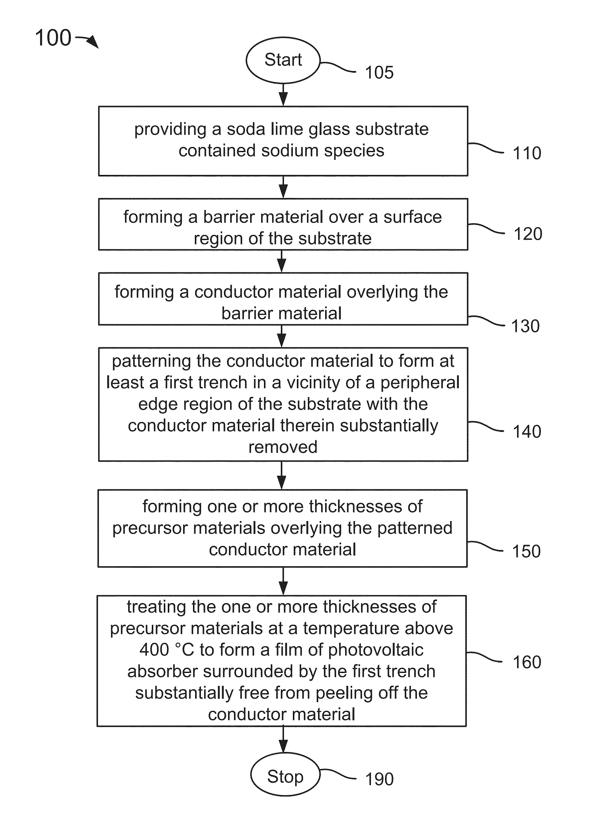
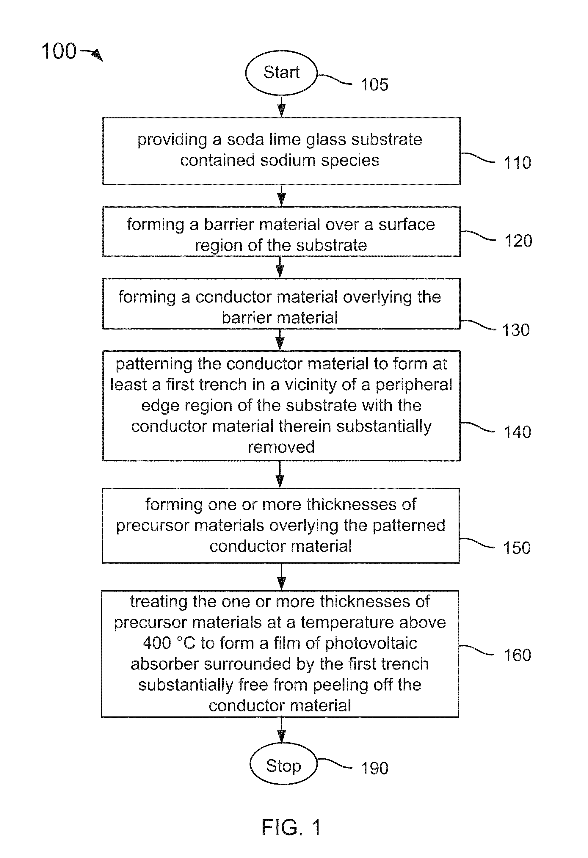
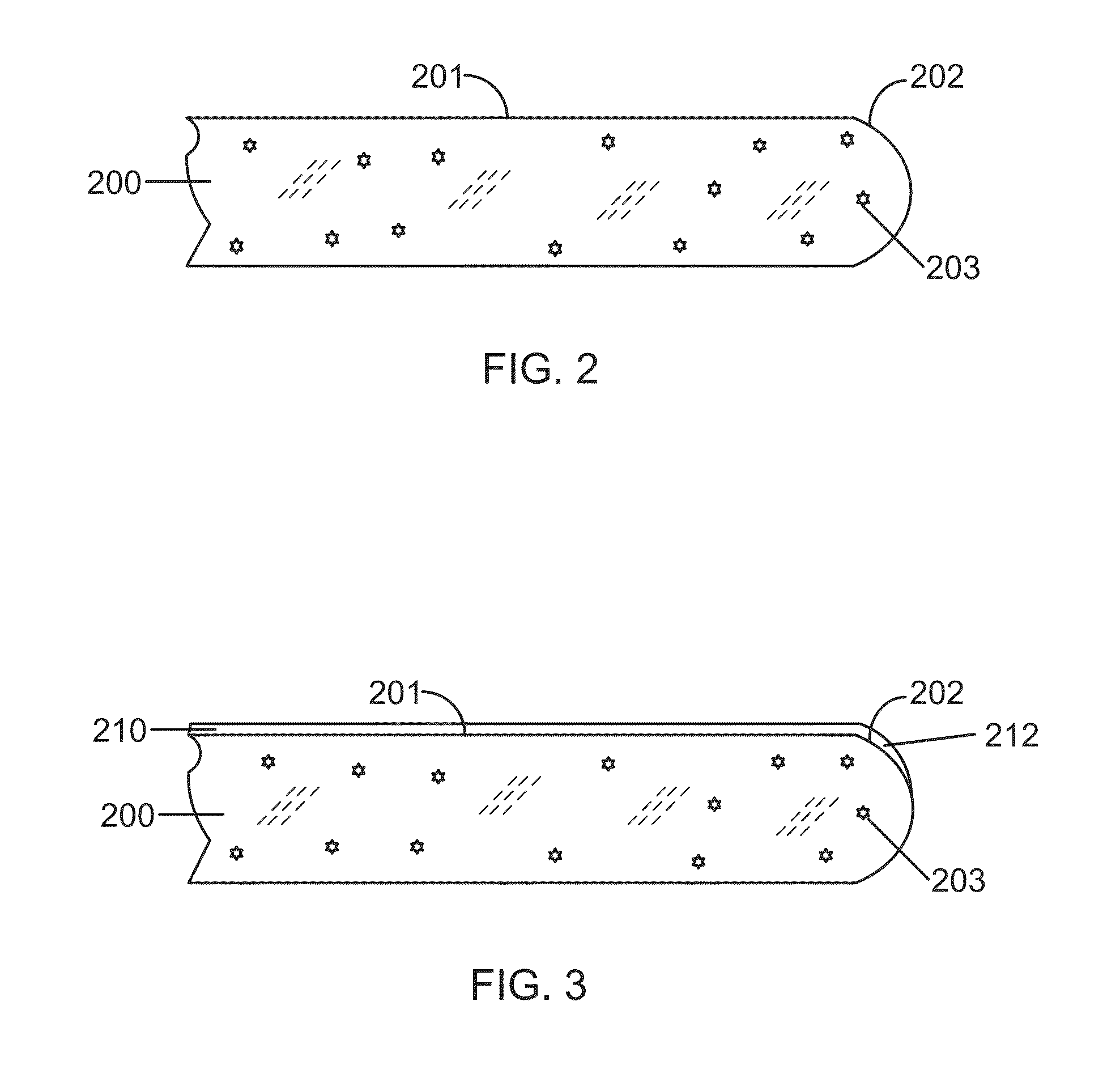
[0013]The present invention relates generally to techniques for the manufacture of photovoltaic devices. More particularly, the present invention provides a method and structure for eliminating peeling of a photovoltaic absorber film from the lower conductive material. Merely by way of examples, the present method includes patterning a conductive film to form a trench structure to isolate peripheral edge region for ensuring the thin-film photovoltaic absorber on main surface region substantially free from peeling off due to impurity from the edge region of the substrate, but it would be recognized that the invention may have other applications.

[0014]Out of various forms, flat glass panels have been widely used as substrates for the manufacture of thin-film photovoltaic modules. A rectangular shaped window glass often is a choice for making monolithic thin-film solar module for being installed on a building roof or being assembled into a solar-energy production system in large-scale ...


PUM

PropertyMeasurementUnit
temperaturesaaaaaaaaaa
widthaaaaaaaaaa
temperatureaaaaaaaaaa

Abstract

A method for manufacturing a thin-film photovoltaic device includes providing a glass substrate contained sodium species. The glass substrate comprising a surface region and a peripheral edge region surround the surface region. The method further includes forming a barrier material overlying the surface region and partially overlying the peripheral edge region and forming a conductor material overlying the barrier material. Additionally, the method includes forming at least a first trench in a vicinity of the peripheral edge region to remove substantially the conductor material therein and forming precursor materials overlying the patterned conductor material. Furthermore, the method includes thermally treating the precursor materials to transform the precursor materials into a film of photovoltaic absorber. The first trench is configured to maintain the film of photovoltaic absorber substantially free from peeling off the conductor material.

Description

BACKGROUND OF THE INVENTION[0001]The present invention relates generally to techniques for the manufacture of photovoltaic devices. More particularly, the present invention provides a method and structure for eliminating peeling of a photovoltaic absorber film from the lower conductive material. Merely by way of examples, the present method is implemented within a routine patterning process for the manufacture of thin-film photovoltaic modules to prevent peeling caused by impurity from edge region of the substrate, but it would be recognized that the invention may have other applications.[0002]From the beginning of time, mankind has been challenged to find way of harnessing energy. Energy comes in the forms such as petrochemical, hydroelectric, nuclear, wind, biomass, solar, and more primitive forms such as wood and coal. Over the past century, modern civilization has relied upon petrochemical energy as an important energy source. Petrochemical energy includes gas and oil. Gas inclu...

Claims


Application Information

Patent Timeline
Patent Type & Authority Applications(United States)
IPC IPC(8): H01L31/0248H01L31/18
CPCH01L31/0248H01L31/18H01L31/03923H01L31/0463Y02E10/541Y02P70/50H01L31/0236
Inventor DOUNAS, LAILAWIETING, ROBERT D.FARRIS, III, CHESTER A.
Owner CM MFG
Why Eureka
Try Eureka