Substrate processing apparatus

a processing apparatus and substrate technology, applied in the field of processing apparatuses, can solve the problems of non-uniform temperature drop, heat accumulation in the cassette (foup) and/or warp of the wafer, etc., and achieve the effect of enhancing the throughput, and reducing the time required for cooling the substra

Active Publication Date: 2013-02-19
TOKYO ELECTRON LTD
View PDF11 Cites 6 Cited by
  • Summary
  • Abstract
  • Description
  • Claims
  • Application Information

AI Technical Summary

Benefits of technology

[0014]The present invention has been made in view of the above circumstances. The object of the present invention is to provide, in a system of a high productivity, a substrate processing apparatus capable of reducing an unnecessary time, having a function for transporting a substrate, and promptly decreasing a high temperature of a substrate to a predetermined temperature.

Problems solved by technology

In this case, there are problems of heat accumulation in the cassette (FOUP) and / or warp of the wafer caused by a non-uniform temperature decrease in the cassette.

Method used


Image

  • Substrate processing apparatus
  • Substrate processing apparatus
  • Substrate processing apparatus

Examples


Embodiment Construction

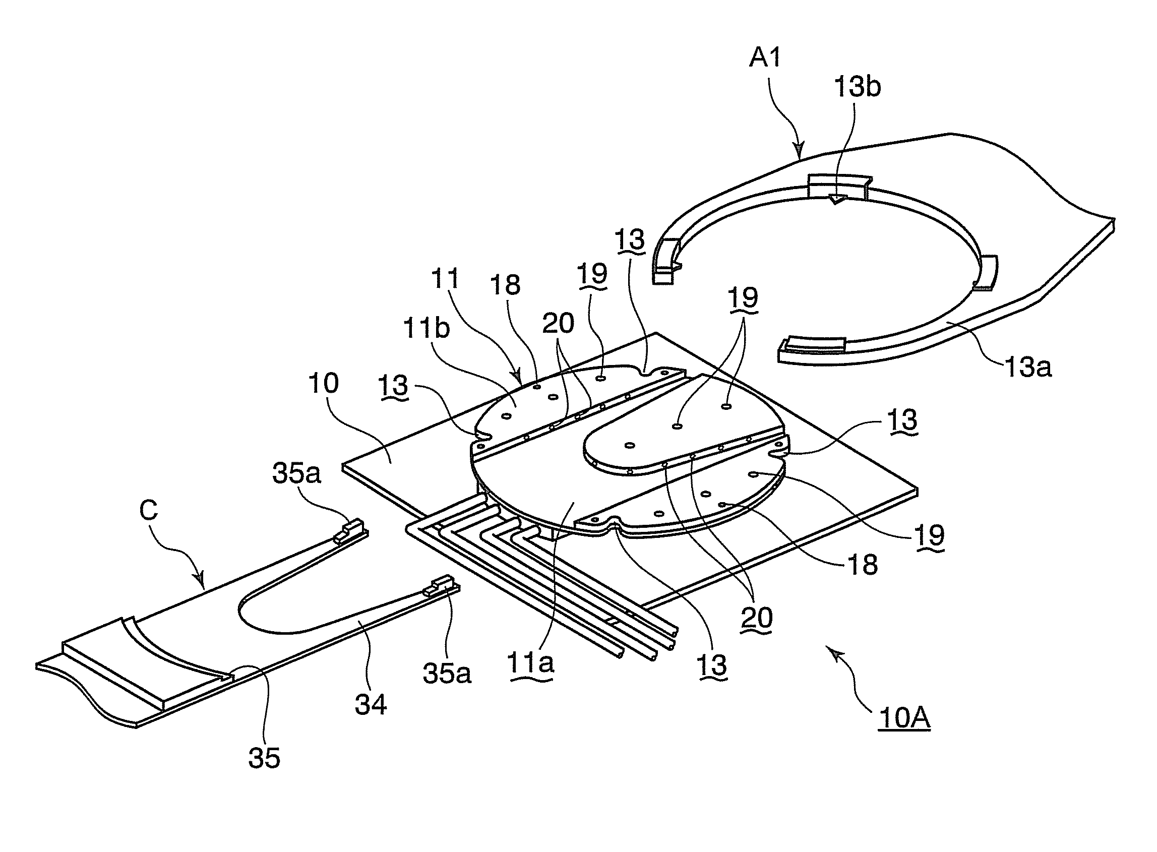
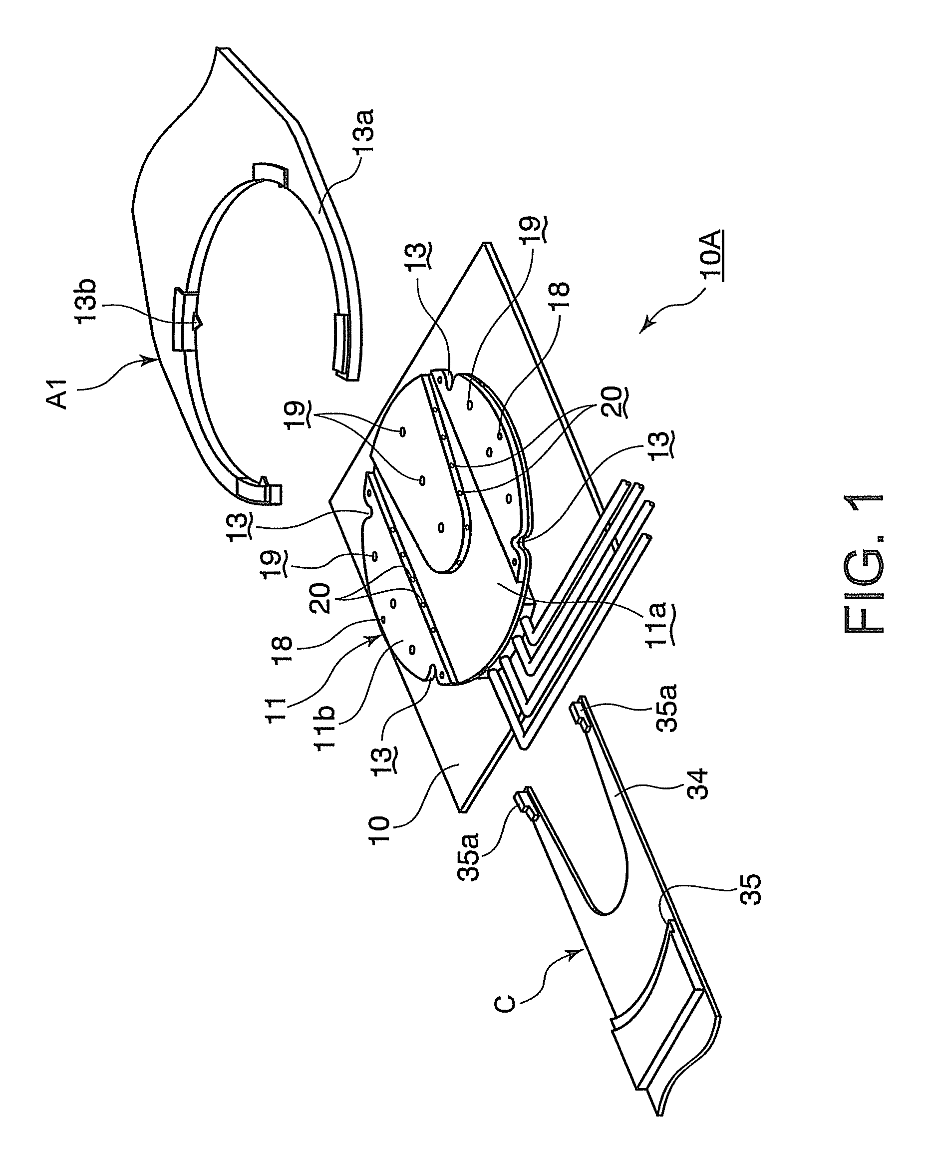
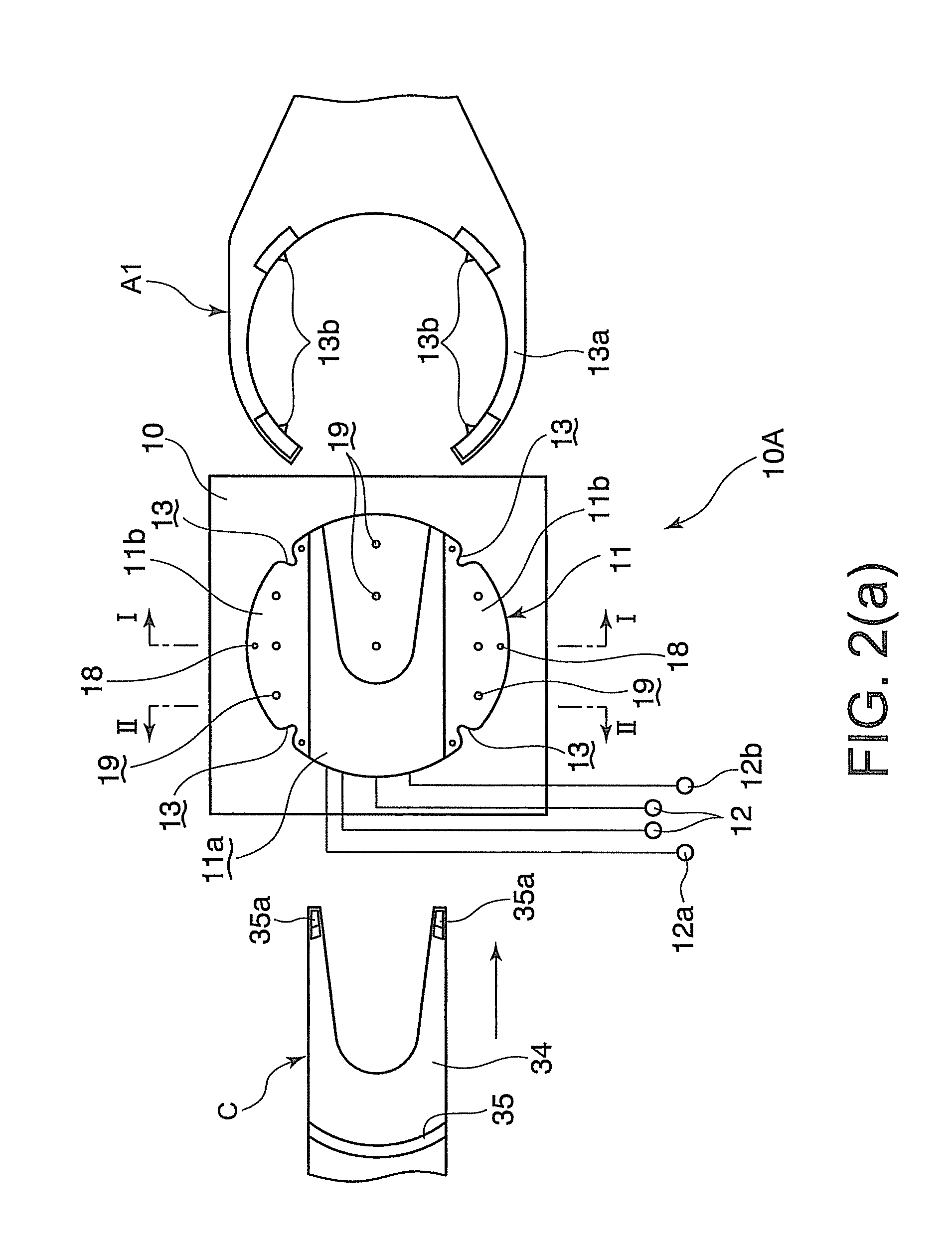
[0046]An embodiment of the present invention will be described herebelow with reference to the attached drawings. Given herein as an example to describe the present invention is a case where a substrate processing apparatus according to the present invention is applied to a coating and developing apparatus for semiconductor wafers.

[0047]As shown in FIGS. 8 and 9, the coating and developing apparatus includes a carrier block S1 provided with a table 80a. From a carrier 80 which is a sealable-type substrate container placed on the table 80a, a transport arm C which is a second substrate transfer means takes out a wafer W and transports the wafer W to a processing block S2. Then, the transport arm C receives a processed wafer W from the processing block S2 and returns the wafer W to the carrier 80.

[0048]As shown in FIG. 8, the processing block S2 includes a first block (DEV layer) B1, a second block (BCT layer) B2, a third block (COT layer) B3, and a fourth block (TCT layer) B4, which ...


PUM


Abstract

A substrate processing apparatus including: a heating part for heating a wafer; a transport part through which a wafer is transported; a first transfer arm that receives a wafer from the heating part and places the wafer on the transport part; and a second transfer arm including a pair of plate-like tweezers that receives the wafer placed on the transport part from the transport part and transfers the wafer. The transport part includes a cooling plate having a cooling surface on which a wafer is placed. The cooling plate includes a temperature-adjusting channel through which a temperature-adjusting water is circulated for cooling the cooling plate to a temperature lower than a temperature of the heating process of the heating part. The cooling surface is provided with a recess that is similar in shape to and slightly larger than a planar shape of the pair of tweezers.

Description

CROSS REFERENCE TO RELATED APPLICATIONS[0001]This application is based upon and claims the benefit of priority from the prior Japanese Patent Application No. 2009-025591 filed on Feb. 6, 2009, the entire contents of which are incorporated herein by reference.FIELD OF THE INVENTION[0002]The present invention relates to a processing apparatus for a substrate such as a semiconductor wafer and a glass substrate (FPD substrate) for liquid crystal display.BACKGROUND ART[0003]A step for forming a resist pattern on a substrate, which is one of processes for manufacturing a semiconductor device and an FPD substrate, is composed of a series of steps in which a resist film is formed on a substrate such as a semiconductor wafer (hereinafter referred to as “wafer”), the resist film is exposed with the use of a photomask, and thereafter a desired pattern is obtained by performing a developing process. These series of steps has been conventionally performed by a coating and developing apparatus.[0...

Claims


Application Information

Patent Timeline
Patent Type & Authority Patents(United States)
IPC IPC(8): B05C13/02
CPCH01L21/67109H01L21/68707H01L21/67748G06F1/20H05K7/20172
Inventor MIZUNAGA, KOUICHI
Owner TOKYO ELECTRON LTD
Why Eureka
Try Eureka