Solid state imaging device

a solid-state imaging and image technology, applied in the direction of semiconductor devices, photovoltaic energy generation, electrical appliances, etc., can solve the problems of reduced image quality of reproduced color images, color mixtures that are required to be suppressed, and difficulty in increasing the pixel density and the sensitivity of solid-state imaging devices, so as to achieve less color mixtures, higher resolution, and high pixel density

Active Publication Date: 2013-02-19
UNISANTIS ELECTRONICS SINGAPORE PTE LTD
View PDF4 Cites 28 Cited by
  • Summary
  • Abstract
  • Description
  • Claims
  • Application Information

AI Technical Summary

Benefits of technology

[0025]The present invention has been made in view of the above-described circumstances, and it is an object of the present invention to realize a solid-state imaging device that achieves a higher pixel density, a higher resolution, less color mixture, and a higher sensitivity.
[0078]According to the present invention, a solid-state imaging device that achieves a higher pixel density, a higher resolution, less color mixture, and a higher sensitivity can be provided.

Problems solved by technology

Accordingly, the fact that it is difficult to form such a pixel structure including the island-shaped semiconductor 30 makes it difficult to increase the pixel density and the sensitivity of a solid-state imaging device.
Since the color mixture reduces the image quality of a reproduced color image, color mixture is required to be suppressed.
However, since part of the light beam diagonally incident to the photodiode region 41 is incident to a pixel adjacent to the pixel of interest, a reduction in the resolution of the solid-state imaging device or color mixture in color imaging cannot be avoided.

Method used


Image

  • Solid state imaging device
  • Solid state imaging device
  • Solid state imaging device

Examples


embodiment 1

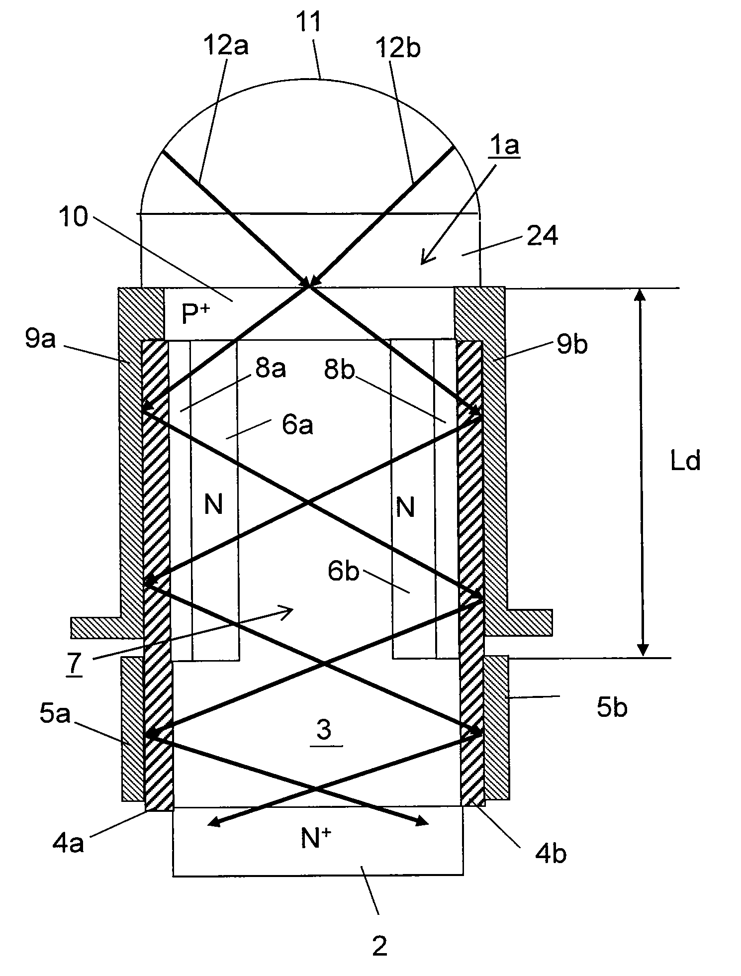
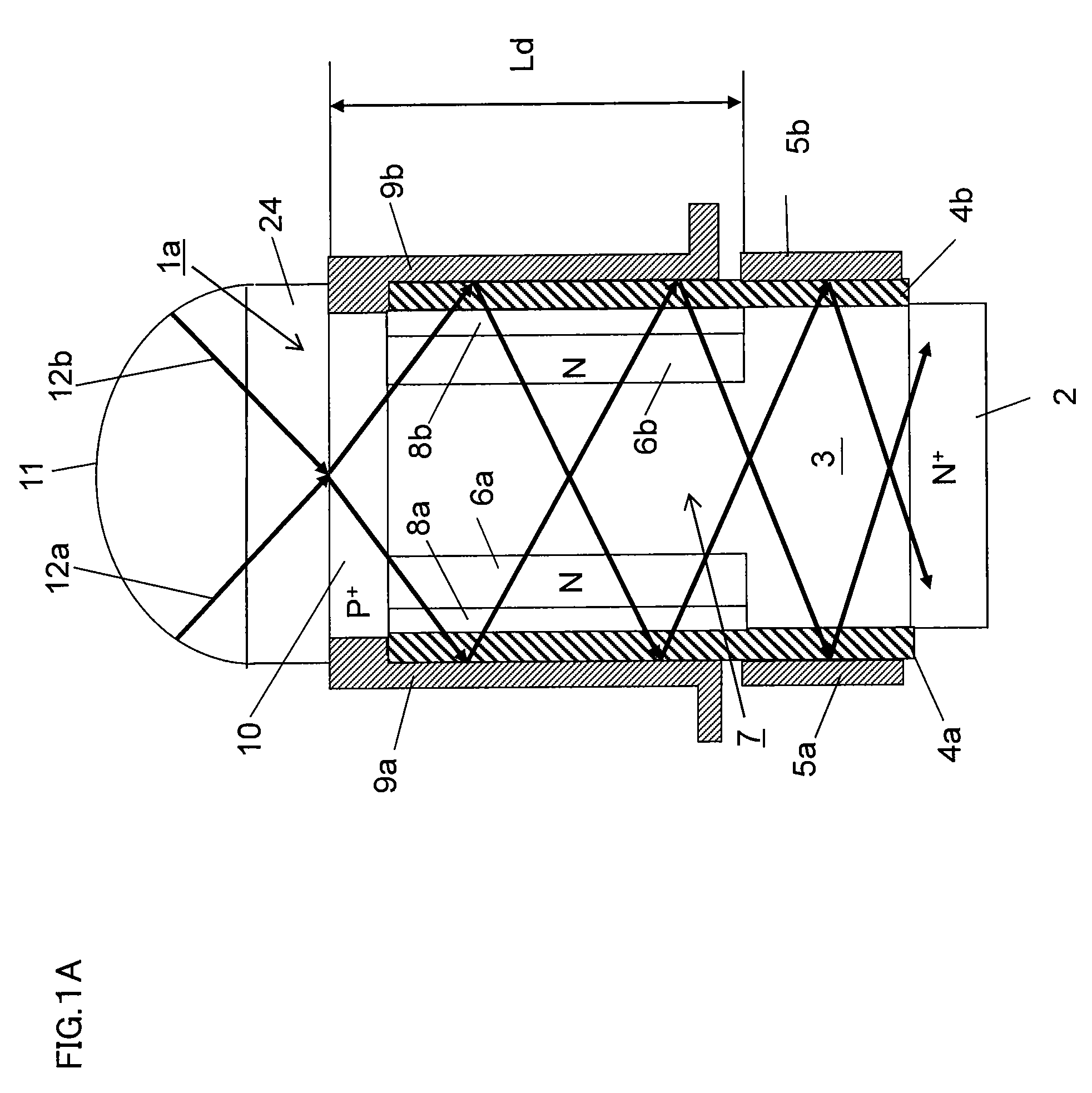
[0111]FIG. 1A illustrates the cross-sectional structure of an island-shaped semiconductor 1a constituting a pixel in a solid-state imaging device according to a first embodiment of the present invention.

[0112]As illustrated in FIG. 1A, a first semiconductor N+-region 2, which is a signal line extending in a first scanning direction in a pixel region on a substrate, is formed so as to extend over the entire lower portion of the island-shaped semiconductor 1a constituting a pixel. On the first semiconductor N+-region 2, a second semiconductor P-region 3 whose conductivity type is opposite to that of the first semiconductor N+-region 2 is formed. On upper lateral sides of the second semiconductor P-region 3, third semiconductor N-regions 6a and 6b whose conductivity type is the same as that of the first semiconductor N+-region 2 are formed.

[0113]Insulating layers 4a and 4b are formed so as to surround the outer periphery of the third semiconductor N-regions 6a and 6b and lower lateral ...

embodiment 2

[0128]FIG. 2A and FIG. 2B illustrate a cross-section diagram and a potential distribution diagram of a solid-state imaging device according to an example of related art. FIG. 2C to FIG. 2F illustrate the pixel structure, potential distribution diagrams, and a schematic plan view of a solid-state imaging device according to a second embodiment of the present invention.

[0129]The solid-state imaging device according to this embodiment not only solves problems relating to a higher pixel density, a higher sensitivity, a reduction in the resolution, and color mixture in color imaging, which are problems of a solid-state imaging device according to related art (see FIG. 12A), but also prevents generation of dark current and dark current noise.

[0130]The cross-sectional structure of the island-shaped semiconductor 30 illustrated in FIG. 2A is the same as the pixel structure illustrated in FIG. 1A with the exception in that, in order to prevent a reduction in the resolution and color mixture ...

embodiment 3

[0163]FIG. 5A and FIG. 5B illustrate the pixel structure of a solid-state imaging device according to a third embodiment of the present invention and the pixel structure of a solid-state imaging device according to a modification of the third embodiment.

[0164]In the solid-state imaging device according to this embodiment illustrated in FIG. 5A, an insulating layer 13 is formed below the island-shaped semiconductor 1a in the solid-state imaging device according to the first embodiment illustrated in FIG. 1A and a light-reflection conductive layer 14a that is made of metal or the like, that reflects light, and that is formed of a conductor is formed below the insulating layer 13. A light beam 12b incident from the upper surface of the microlens 11 is reflected by the light-reflection conductive layers 9a and 9b and the gate conductive layers 5a and 5b and is propagated below the island-shaped semiconductor 1a. A light beam 12c incident to the insulating layer 13 is reflected by the li...


PUM


Abstract

An island-shaped semiconductor constituting a pixel includes a first semiconductor N+-region formed on a substrate, a second semiconductor P-region formed on the region, third semiconductor N-regions formed on upper lateral sides of the region, insulating layers formed on the outer periphery of the regions and lower lateral sides of the region, gate conductive layers formed on the outer periphery of the insulating layers and functioning as gate electrodes forming a channel in a lower area of the region, light-reflection conductive layers formed on the outer periphery of the N regions and a portion of the insulating layers where the gate conductive layers are not formed, a fifth semiconductor P+-region formed on the region and the regions, and a microlens formed on the region and whose focal point is located near the upper surface of the region.

Description

RELATED APPLICATIONS[0001]This application claims the benefit of the filing date of U.S. Provisional Application Ser. No. 61 / 408,131 filed on Oct. 29, 2010 pursuant to 35 U.S.C. §119(e). The entire content of this application is hereby incorporated by reference.BACKGROUND OF THE INVENTION[0002]1. Field of the Invention[0003]The present invention relates to solid-state imaging devices, and more particularly, to a solid-state imaging device that achieves a higher pixel density, a higher resolution, less color mixture, and a higher sensitivity.[0004]2. Description of the Related Art[0005]At present, CCDs and CMOS solid-state imaging devices are widely used in video cameras, still cameras, and the like. Performance improvements in solid-state imaging devices, such as an increase in the pixel density, an increase in the resolution, a reduction in color mixture in color imaging, and an increase in the sensitivity, are always demanded. Under such circumstances, in order to realize a higher...

Claims


Application Information

Patent Timeline
Patent Type & Authority Patents(United States)
IPC IPC(8): H01L31/0232
CPCH01L27/14629H01L31/022416H01L31/02327H01L31/035281H01L31/103H01L27/14627Y02E10/50
Inventor MASUOKA, FUJIOHARADA, NOZOMU
Owner UNISANTIS ELECTRONICS SINGAPORE PTE LTD
Why Eureka
Try Eureka