Method of evaluating a semiconductor storage device

a semiconductor storage device and semiconductor technology, applied in the field of semiconductor storage device evaluation, can solve the problems of deterioration of tunnel insulating film, inability to recognize insulating film, and inability to store data

Inactive Publication Date: 2013-03-19
KK TOSHIBA
View PDF2 Cites 1 Cited by
  • Summary
  • Abstract
  • Description
  • Claims
  • Application Information

AI Technical Summary

Problems solved by technology

However, if the charges are moved in the tunnel insulating film, the tunnel insulating film is deteriorated (trap is generated).
Thereby, the charges are accumulated in the trap that is generated in the tunnel insulating film and a data retention characteristic is deteriorated.
In the conventional art, a charge distribution in the tunnel insulating film cannot be recognized and it is difficult to investigate a quality of the tunnel insulating film or grasp a characteristic of an electron density distribution.

Method used


Image

  • Method of evaluating a semiconductor storage device
  • Method of evaluating a semiconductor storage device
  • Method of evaluating a semiconductor storage device

Examples


first embodiment

[0029]First, the configuration of a NAND-type flash memory that is an example of a floating gate type EEPROM (semiconductor storage device) where a method of evaluating a semiconductor storage device according to the embodiment is applied will be described.

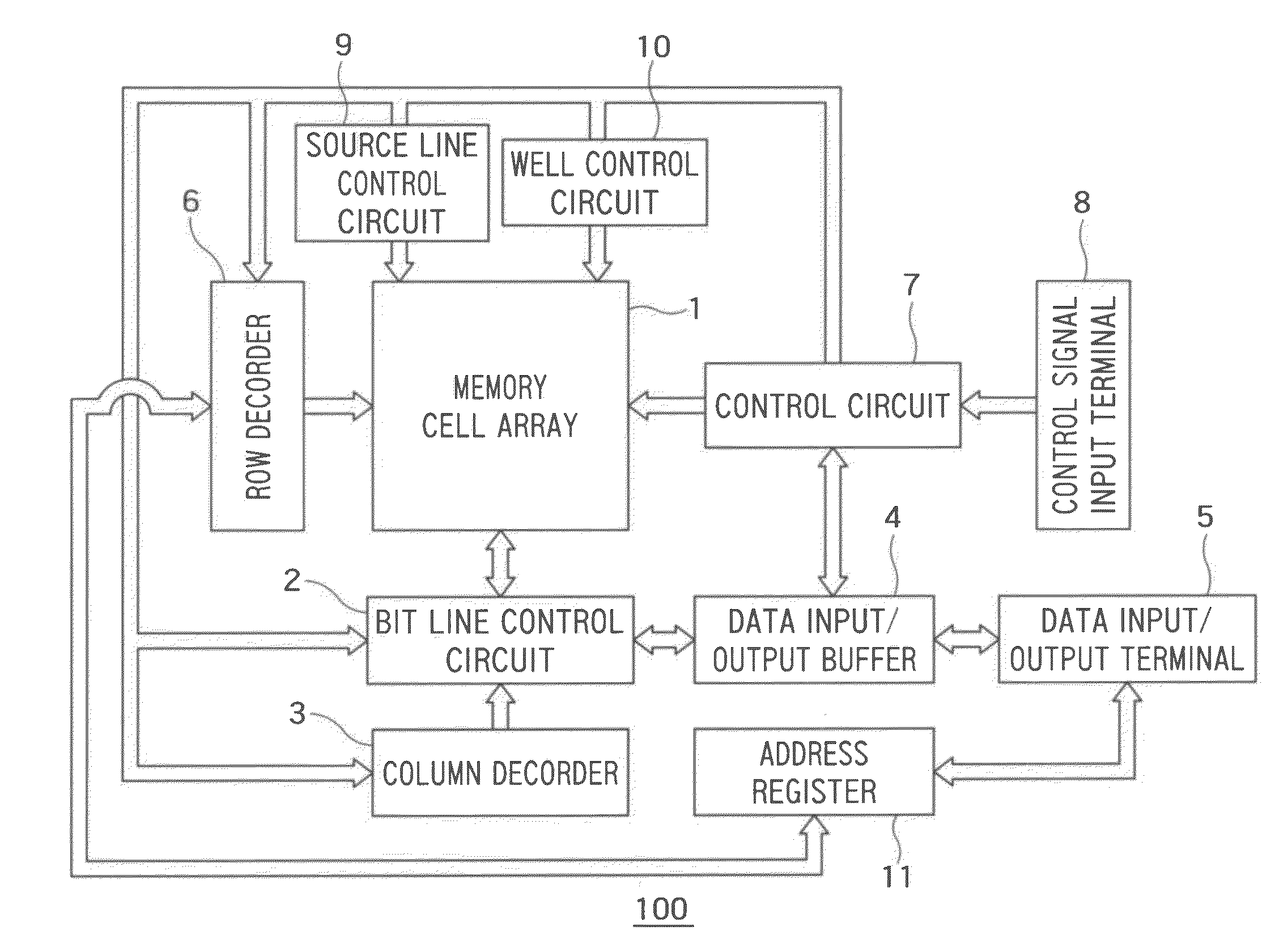
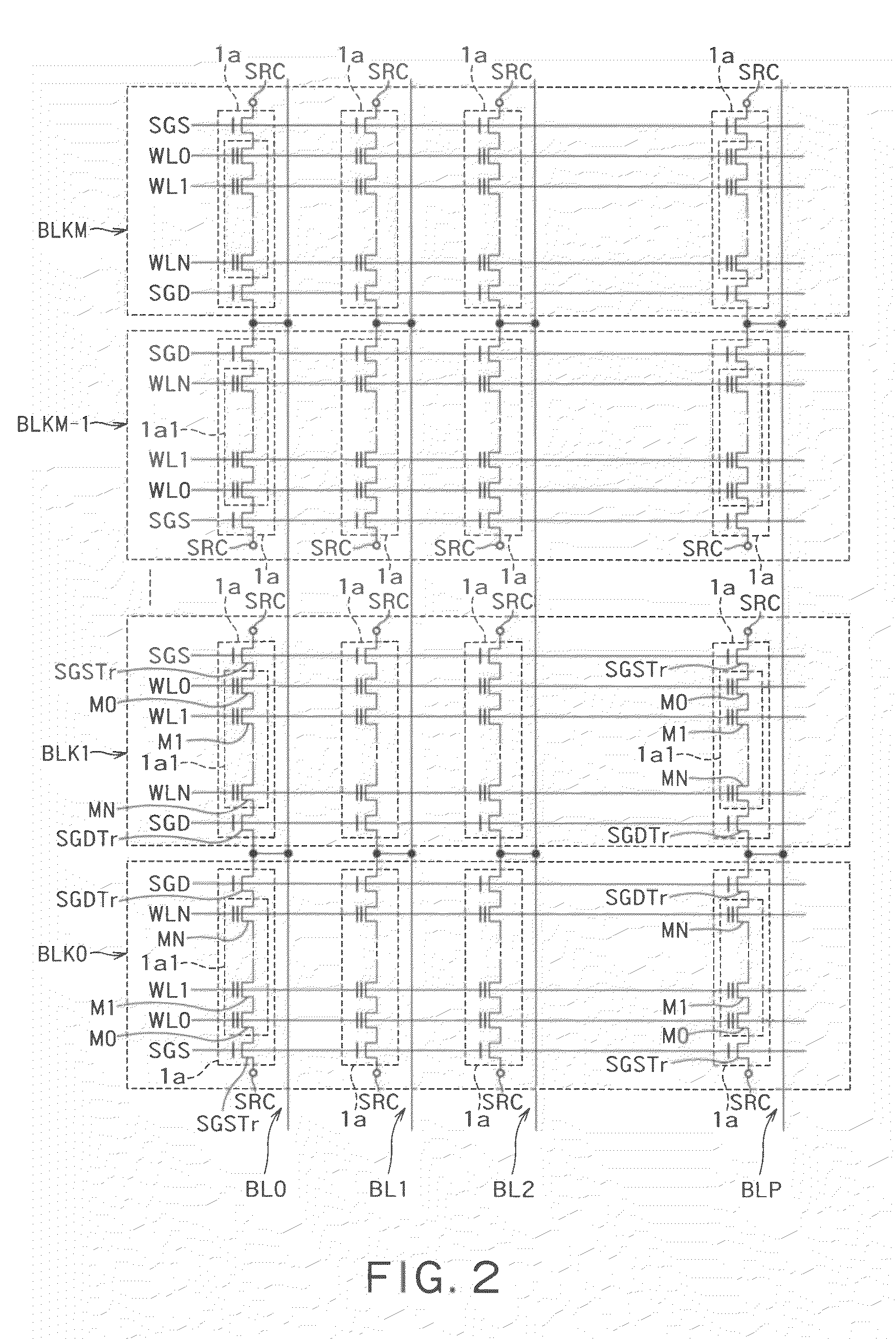
[0030]FIG. 1 is a block diagram showing an example of the configuration of a NAND-type flash memory 100. FIG. 2 is a circuit diagram showing an example of the configuration according to the first embodiment that includes a memory cell array 1, a bit line control circuit 2, and a row decoder 6 shown in FIG. 1.

[0031]As shown in FIG. 1, the NAND-type flash memory 100 includes a memory cell array 1, a bit line control circuit 2, a column decoder 3, a data input / output buffer 4, a data input / output terminal 5, a row decoder 6, a control circuit 7, a control signal input terminal 8, a source line control circuit 9, a well control circuit 10, and an address register.

[0032]The memory cell array 1 includes a plurality of bit lines, a plura...

second embodiment

[0078]In a second embodiment, an example of a method of evaluating a semiconductor storage device to obtain an electron density distribution of a wider range will be described.

[0079]FIG. 7 shows an example of an actual measurement value of the change of the threshold voltage in the case where the memory cells are left at the temperature of 25° C. after a write / erase operation is performed on the memory cells. FIG. 8 shows an example of a change rate ΔVt / ΔIn(t) of the threshold voltage in the case where the memory cells are left at the temperature of 25° C. after a write / erase operation is performed on the memory cells. FIG. 9 shows an example of an actual measurement value of the change of the threshold voltage in the case where the memory cells are left at the temperature of 40° C. after a write / erase operation is performed on the memory cells. FIG. 10 shows an example of a change rate ΔVt / ΔIn(t) of the threshold voltage in the case where the memory cells are left at the temperatur...

third embodiment

[0094]In a third embodiment, a method of calculating a detailed (high-resolution) electron density distribution and an example thereof will be described.

[0095]According to the detailed calculation of the above-described TFM, the existence probability P(x, t) of the electrons that have the small electric field and exist around the surface of the tunnel insulating film with the distance x from the surface of the tunnel insulating film is represented by the following Equation (6) as a function of the time t and the distance x.

P(x,t)=exp(−A*t*exp(−2kx))  (6)

[0096]In the Equation (6), A is a constant that is related to a frequency (attempt frequency) of the electrons tunneling the tunnel insulating film.

[0097]In this case, a curve line of the function shown in the Equation (6) for each lap time selected such that the logarithm of the time is an equivalent interval D=In(t(i+1))−In(ti) is calculated. FIG. 16 shows a curve line showing an example of a relationship between the existence prob...


PUM


Abstract

A method of evaluating a semiconductor storage device of a floating gate type has calculating an electron density distribution of a tunnel insulating film of a memory cell by multiplying a change rate of a threshold voltage Vt of the memory cell of the semiconductor storage device with respect to the change of the logarithm of a time with ε*Cr*2k / Tox / q (where ε is the permittivity of the tunnel insulating film of the memory cell, Cr indicates a coupling ratio of the memory cell, Tox indicates the thickness of the tunnel insulating film, k indicates an attenuation rate of the existence probability when the charges are detrapped and is represented as k=(2mE / (h / 2π)2)0.5, m indicates the mass of the electron, E indicates an energy level of the trap of the tunnel insulating film, h indicates a Planck's constant, and π indicates a circumference ratio).

Description

CROSS-REFERENCE TO RELATED APPLICATION[0001]This application is based upon and claims the benefit of priority from the prior Japanese Patent Application No. 2010-220397, filed on Sep. 30, 2010, the entire contents of which are incorporated herein by reference.BACKGROUND[0002]1. Field[0003]Embodiments described herein relate generally to a method of evaluating a semiconductor storage device.[0004]2. Background Art[0005]For example, a semiconductor storage device of a floating gate type EEPROM such as a NAND-type flash memory makes charges pass through a tunnel insulating film and changes the charge amount of a floating gate.[0006]However, if the charges are moved in the tunnel insulating film, the tunnel insulating film is deteriorated (trap is generated). Thereby, the charges are accumulated in the trap that is generated in the tunnel insulating film and a data retention characteristic is deteriorated.[0007]In the conventional art, a charge distribution in the tunnel insulating film...

Claims


Application Information

Patent Timeline
Patent Type & Authority Patents(United States)
IPC IPC(8): G11C16/04
CPCG11C16/0466G11C29/50004G11C29/50016G11C16/00
Inventor MATSUKAWA, NAOHIRO
Owner KK TOSHIBA
Why Eureka
Try Eureka