Method for producing a micromechanical component having a filler layer and a masking layer

a technology of filler layer and masking layer, applied in the direction of microelectromechanical systems, microstructural devices, microstructural technology, etc., can solve the problems of cap wafers that must be laboriously patterned and complete filling

Inactive Publication Date: 2013-04-16
ROBERT BOSCH GMBH
View PDF20 Cites 0 Cited by
  • Summary
  • Abstract
  • Description
  • Claims
  • Application Information

AI Technical Summary

Benefits of technology

[0005]The method according to the present invention in accordance with the main claim or with the features of the coordinated claims has, in contrast thereto, the advantage that even large trench structures can be substantially completely filled up in uncomplicated fashion by way of a first filler layer, and filler layers can simultaneously be used as a functional layer. By way of the functional layer, spacing elements can be formed to protect the movable sensor structures from contact with a cap wafer. For formation of the spacing elements, in the method for producing the micromechanical component a second filler layer is applied over the first filler layer having the first mask layer, and a second mask layer is applied over that. The first mask layer is thus “buried” under the second filler layer, with the result that, advantageously, in the context of an etching operation the first mask layer acts as a stop layer, so that the material (first filler layer and substrate material) located under the first mask layer is substantially not removed by the etching operation.
[0010]The second filler layer is preferably planarized, proceeding from the first side of the substrate material, prior to application of the second mask layer. Here as well, a plane surface of the second filler layer is advantageously formed, with the result that the second mask layer as well can advantageously be applied onto the second filler layer substantially in one plane parallel to the main extension direction of the substrate material.
[0014]A cap wafer is preferably connected to the spacing element and / or to monocrystalline or polycrystalline regions of the filler layers, for example by anodic bonding or seal-glass bonding. It is also preferred, however, if the cap wafer is connected to at least one (preliminary, non-movable) sensor structure and / or to monocrystalline or polycrystalline regions of the filler layers. If the micromechanical component does not have a spacing element, the sensor structures are therefore advantageously not only thought of as precursors of the movable sensor structures, but additionally serve to reduce cap deflection in the region of the movable sensor structures. In the case of a micromechanical component without a spacing element, care must be taken in the context of the connection between an unpatterned cap wafer and the sensor structure that the movable sensor structures are not blocked by the unpatterned cap wafer. This can be ensured by using a connecting layer, for example seal glass. The necessary spacing from the movable sensor structures can be ensured by way of the thickness of the seal-glass layer. Let it be clarified once again in this context that the sensor structure for connecting to the cap wafer is not a movable sensor structure, but instead a (preliminary) sensor structure that has not become a movable sensor structure as a result of a further etching step. A “cap wafer” is to be understood as all components that can be used to seal off at least subregions of a micromechanical component. The spacing element or sensor structure having, for example, seal-glass-bonded cap wafers advantageously makes it possible also to use unpatterned cap wafers, so that laborious patterning of the cap wafer is eliminated. Especially in the context of the use of a spacing element, laborious patterning of, for example, Pyrex cap wafers prior to anodic bonding is no longer necessary. It is of course also possible, however, to use patterned cap wafers or even cap wafers patterned only in subregions, the patterning of the cap wafer enabling, for example, electrical contacting of the micromechanical component.
[0015]The cap wafer and / or a second side of the substrate material is preferably planarized. In the context of planarization of the second side of the substrate material, a planarization extending into a plane of the trench structure is advantageously performed. Planarization of the cap wafer and / or of the second side of the substrate material advantageously makes the micromechanical component thinner. In addition, planarization of the second side of the substrate material extending into a plane of the trench structure advantageously makes possible back-side contacting of the micromechanical component.
[0017]The cap wafer is preferably connected via anodic bonding or seal-glass bonding to the spacing element and / or to the monocrystalline or polycrystalline regions of the filler layers. The spacing element is constituted in this context by the first and the second filler layer, and has a greater height than the movable sensor structure or the sensor structure. As a result of the greater height as compared with the movable sensor structure, the cap wafer can advantageously be connected to the spacing element directly by anodic bonding, with no need to perform patterning of the cap wafer and no interference with the movable sensor structures as a result of contact with the cap wafer. The spacing element thus advantageously makes possible anodic bonding between the cap wafer and the micromechanical component without patterning the cap wafer.
[0020]The micromechanical component is preferably planarized proceeding from a first side of the substrate material and / or from a second side of the substrate material. Planarization advantageously makes the micromechanical component thinner so that it can be better incorporated even into flat assemblies.

Problems solved by technology

A disadvantage of the known micromechanical components, however, is that large trench structures in particular cannot as a rule be completely filled up, and moreover that in the case of a micromechanical component having movable sensor structures, cap wafers must be laboriously patterned so that the cap wafers are spaced away from the movable sensor structures.

Method used


Image

  • Method for producing a micromechanical component having a filler layer and a masking layer
  • Method for producing a micromechanical component having a filler layer and a masking layer
  • Method for producing a micromechanical component having a filler layer and a masking layer

Examples


Embodiment Construction

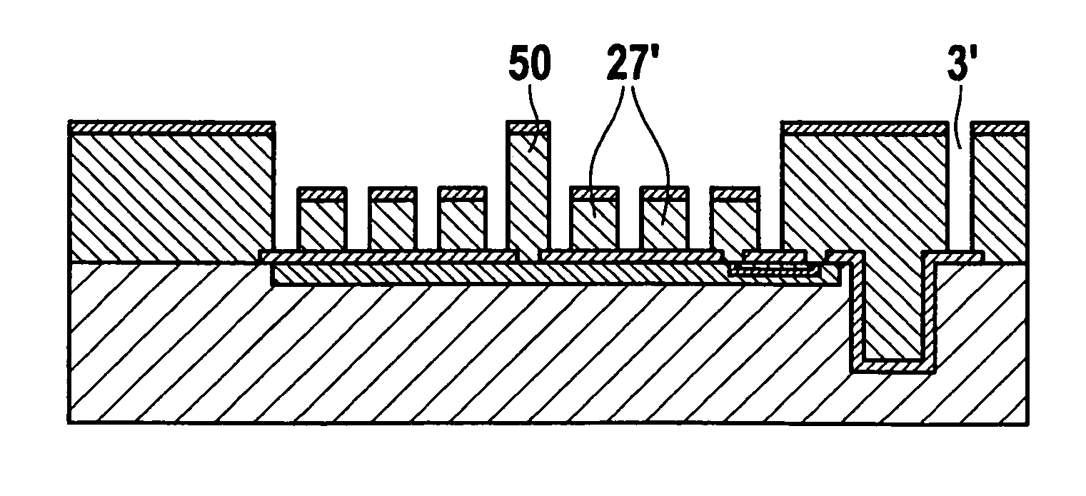
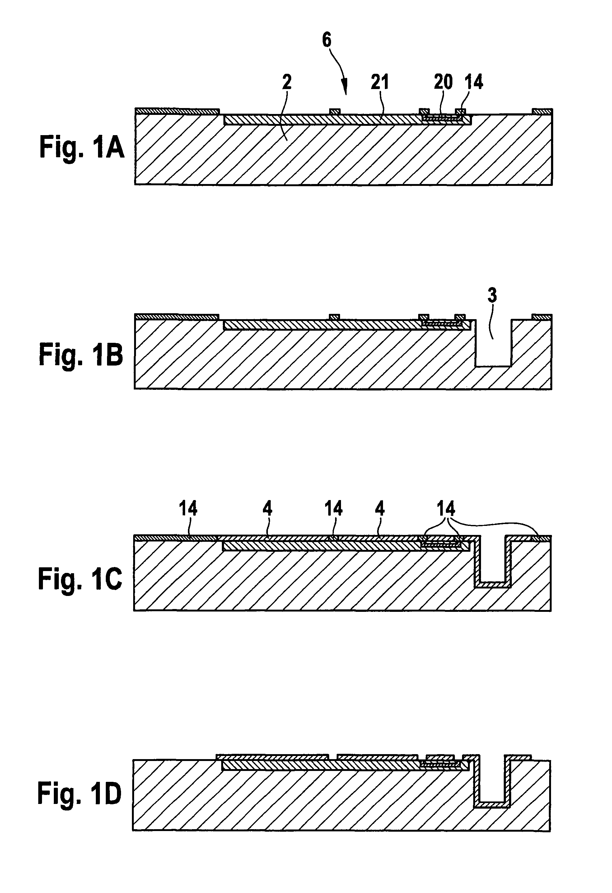
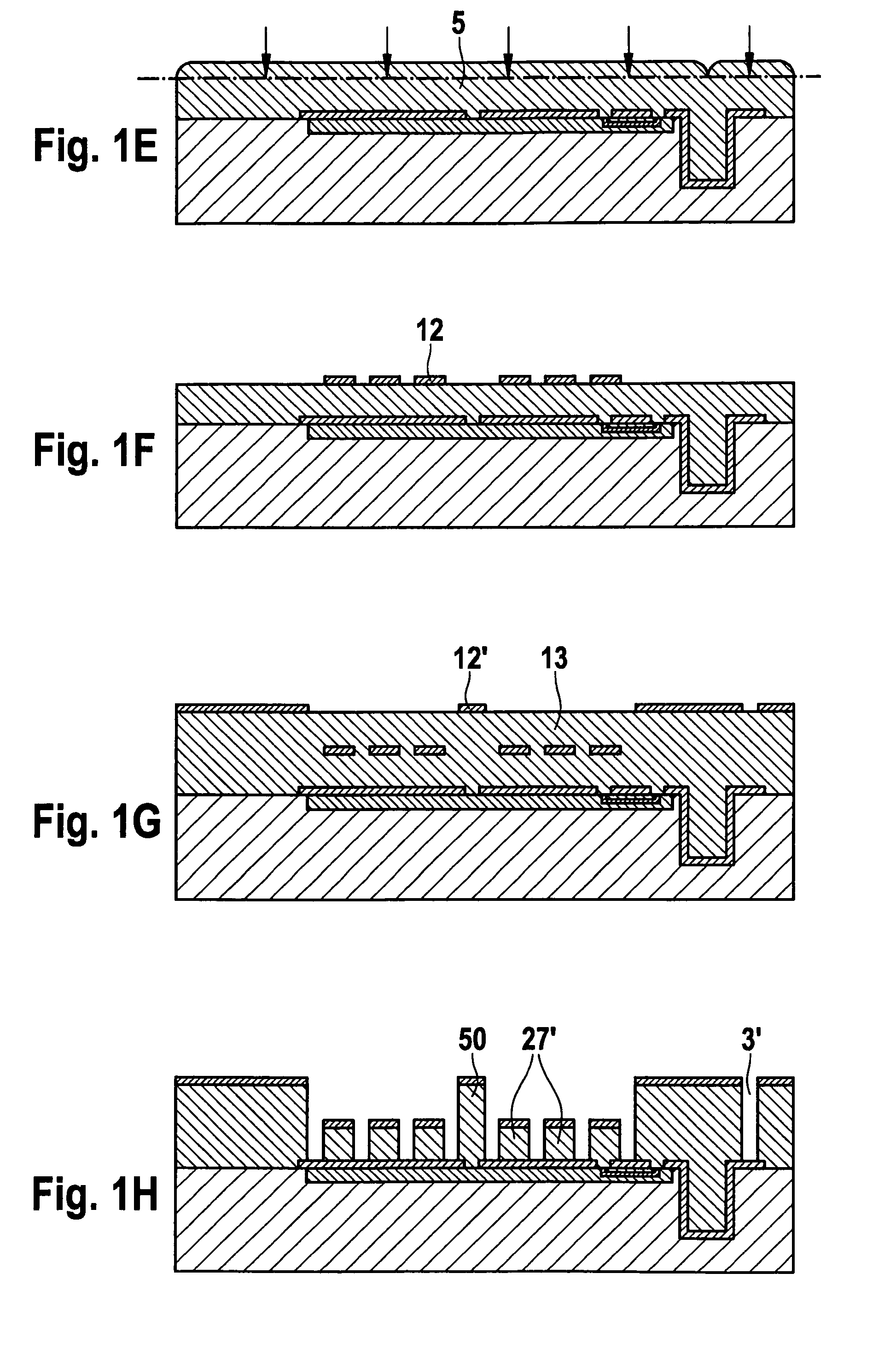
[0024]FIG. 1A schematically depicts a substrate material 2, for example silicon, having a circuit region 21 and a conductive path 20. A third mask layer 14, made e.g. of silicon nitride, is applied on a first side 6 of substrate material 2. FIG. 1B schematically depicts the manner in which a trench structure 3 was produced in substrate material 2. By way of a subsequent (e.g. LOCOS) process, a first insulating layer 4 is deposited on substrate material 2, the walls and floor of trench structure 3 being covered by first insulating layer 4 (FIG. 1C). The regions in which third mask layer 14 were applied remain free of third insulating layer 4, however. After the removal of third mask layer 14, for example by way of an etching step, gaps are created in first insulating layer 4 (FIG. 1D). Both these gaps and first trench structure 3 are filled up by a first filler layer 5 that is made, for example, of doped silicon (FIG. 1E); first filler layer 5 can grow in monocrystalline fashion into...


PUM

PropertyMeasurementUnit
electrical resistanceaaaaaaaaaa
heightaaaaaaaaaa
structureaaaaaaaaaa

Abstract

A method for producing a micromechanical component is proposed, a trench structure being substantially completely filled up by a first filler layer, and a first mask layer being applied on the first filler layer, on which in turn a second filler layer and a second mask layer are applied. A micromechanical component is also proposed, the first filler layer filling up the trench structure of the micromechanical component and at the same time forming a movable sensor structure.

Description

BACKGROUND OF THE INVENTION[0001]1. Field of the Invention[0002]The present invention relates to a method for producing micromechanical components having trench structures commonly known from German Published Application DE 2004 036 035.[0003]2. Description of Related Art[0004]A disadvantage of the known micromechanical components, however, is that large trench structures in particular cannot as a rule be completely filled up, and moreover that in the case of a micromechanical component having movable sensor structures, cap wafers must be laboriously patterned so that the cap wafers are spaced away from the movable sensor structures.SUMMARY OF THE INVENTION[0005]The method according to the present invention in accordance with the main claim or with the features of the coordinated claims has, in contrast thereto, the advantage that even large trench structures can be substantially completely filled up in uncomplicated fashion by way of a first filler layer, and filler layers can simu...

Claims


Application Information

Patent Timeline
Patent Type & Authority Patents(United States)
IPC IPC(8): C03C15/00
CPCB81C1/0015B81C1/00333B81B2203/033B81C2201/0197
Inventor SCHEUERER, ROLANDWEBER, HERIBERTGRAF, ECKHARD
Owner ROBERT BOSCH GMBH
Why Eureka
Try Eureka