
Method for manufacturing semiconductor device and semiconductor device

a manufacturing method and semiconductor technology, applied in semiconductor lasers, semiconductor devices, electrical devices, etc., can solve the problems of difficult to obtain the nitride-based iii-v compound semiconductor layer having a flat surface, unwound processing, etc., and achieve good crystallinity and good crystallinity. , the effect of flat surfa

Inactive Publication Date: 2013-05-07
SONY CORP
View PDF1 Cites 0 Cited by
  • Summary
  • Abstract
  • Description
  • Claims
  • Application Information

AI Technical Summary

Benefits of technology

The present invention relates to a method of manufacturing a semiconductor device using nitride-based III-V compound semiconductor layers. The invention aims to solve the difficulty in obtaining a nitride-based III-V compound semiconductor layer with good crystallinity and a flat surface without the need for a buffer layer. By properly selecting the surface orientation of the substrate and the thickness of the low-temperature GaN buffer layer, a very thin low-temperature GaN buffer layer can be grown, achieving good crystallinity and a flat surface. This semiconductor device can be used in various electronic apparatuses such as displays and lighting devices.

Problems solved by technology

Growing the buffer layer before the growth of the nitride-based III-V compound semiconductor layer forming the device structure, as mentioned above, increases the number of steps for manufacturing a semiconductor device, and hence such a process is not desired from the viewpoint of simplifying the manufacturing steps.
Under the present situation, however, there is a difficulty in obtaining the nitride-based III-V compound semiconductor layer having a flat surface and good crystallinity by growing the nitride-based III-V compound semiconductor layer, which forms the device structure, without growing the buffer layer.

Method used


Image

  • Method for manufacturing semiconductor device and semiconductor device
  • Method for manufacturing semiconductor device and semiconductor device
  • Method for manufacturing semiconductor device and semiconductor device

Examples


first embodiment

[Method for Manufacturing Semiconductor Device and Semiconductor device]

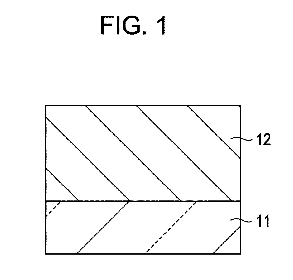
[0077]In a first embodiment, as illustrated in FIG. 1, a sapphire substrate 11 having a principal surface, which is oriented off at an angle of not less than −0.5° and not more than 0° from an R-plane with respect to the direction of a C-axis, is prepared and the surface of the sapphire substrate 11 is cleaned by thermal cleaning, for example, with a usual method.

[0078]Next, a nitride-based III-V compound semiconductor layer 12 forming a device structure is grown directly on the cleaned surface of the sapphire substrate 11 without growing a buffer layer. For example, an MOCVD process is used to grow the nitride-based III-V compound semiconductor layer 12.

[0079]Growth conditions of the nitride-based III-V compound semiconductor layer 12 are, for example, as follows. The growth rate is 0.5 to 8 μm / hour, the flow rate of a III element material (such as trimethylgallium ((CH3)3Ga, TMG), trimethylaluminum ((CH3)3Al, ...

example 1

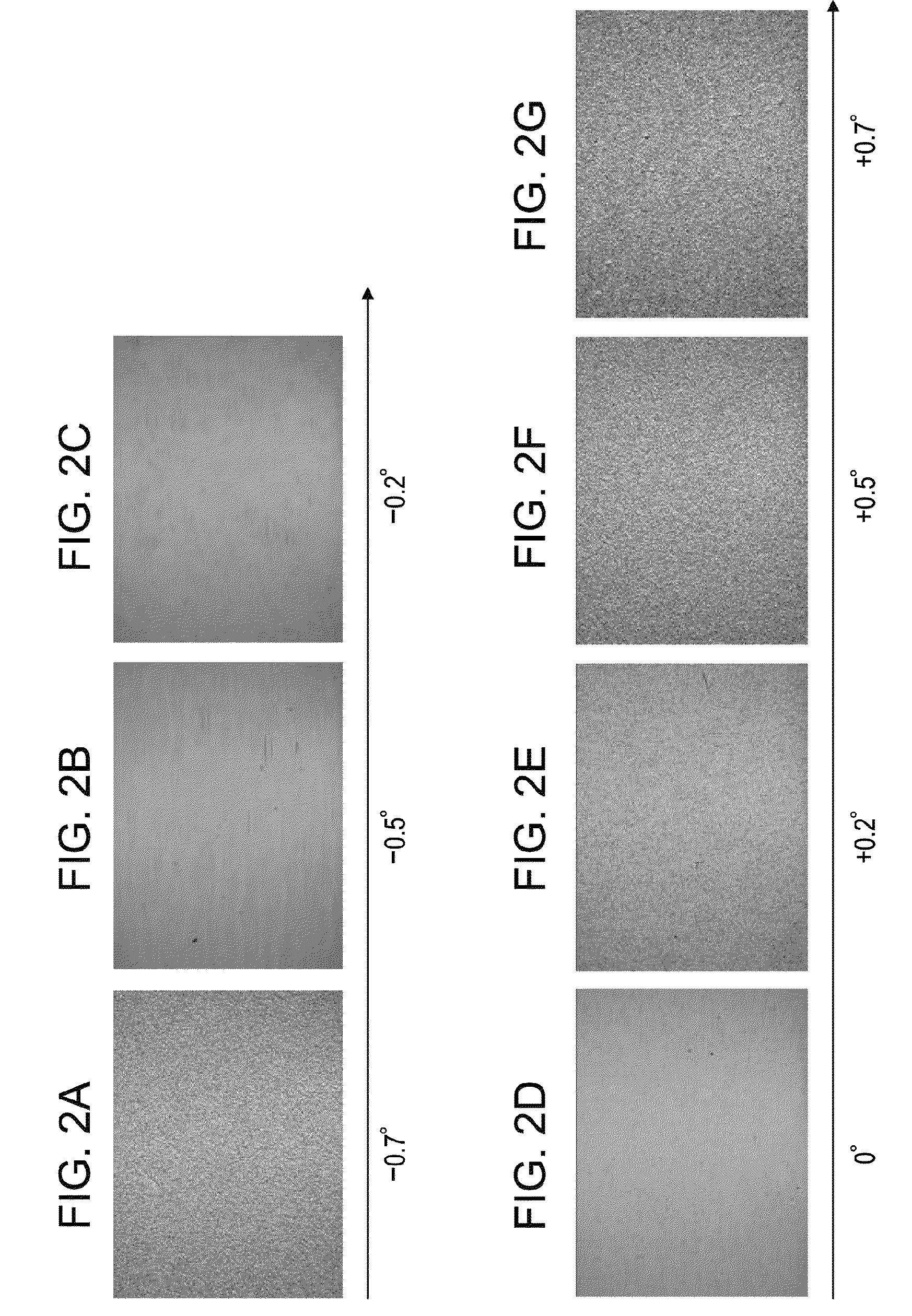
[0083]Sapphire substrates 11 having off-angles changed in seven levels, i.e., −0.7°, −0.5°, −0.2°, 0°, +0.2°, +0.5° and +0.7°, relative to the R-plane were prepared. Then, samples were fabricated by directly growing a GaN layer in a thickness of 3.5 μm on each of the prepared sapphire substrates 11 with the MOCVD process without growing a buffer layer.

[0084]FIGS. 2A to 2G represent optical microscope images (bright field images) (×5) of surfaces of the samples prepared by growing the GaN layers directly on the sapphire substrates 11, which have the off-angles of −0.7°, −0.5°, −0.2°, 0°, +0.2°, +0.5° and +0.7°, without forming the buffer layer. Further, FIGS. 3A to 3G represent optical microscope images (bright field images) (×100) of surfaces of the samples prepared by growing the GaN layers directly on the sapphire substrates 11, which have the off-angles of −0.7°, −0.5°, −0.2°, 0°, +0.2°, +0.5° and +0.7°, without forming the buffer layer. As seen from FIGS. 2A to 2G and FIGS. 3A t...

second embodiment

[Light Emitting Diode and Method for Manufacturing the Same]

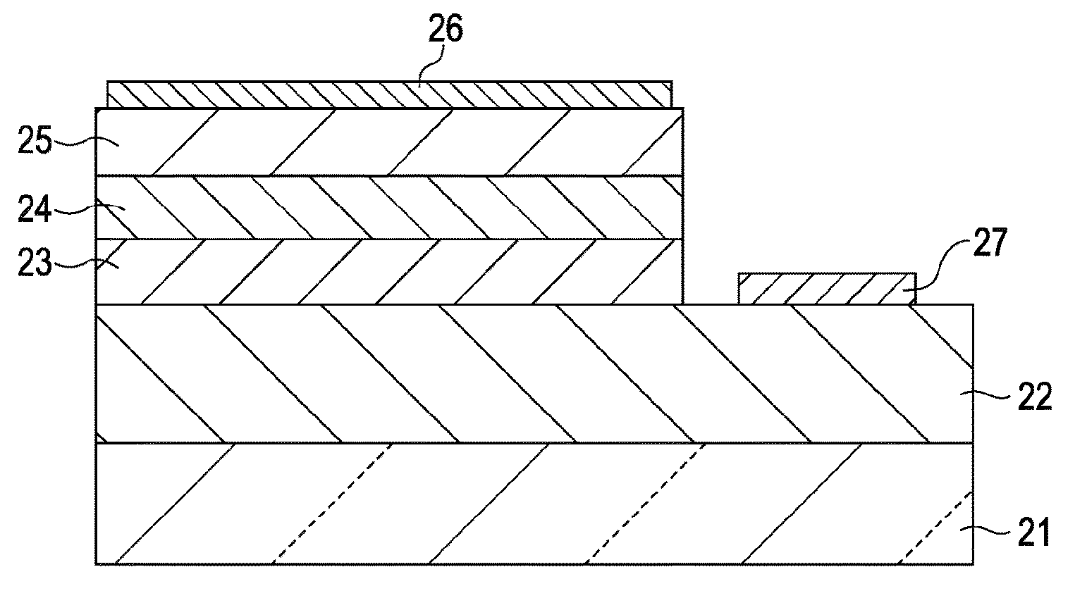
[0089]In a second embodiment, as illustrated in FIG. 6, a sapphire substrate 21 having a principal surface, which is oriented off at an angle of not less than −0.5° and not more than 0° from an R-plane with respect to the direction of a C-axis, is prepared and the surface of the sapphire substrate 21 is cleaned by thermal cleaning, for example, with a usual method.

[0090]Next, a nitride-based III-V compound semiconductor layer forming a light emitting diode structure is grown directly on the cleaned surface of the sapphire substrate 21 without growing a buffer layer. More specifically, by way of example, an n-type nitride-based III-V compound semiconductor layer 22, another n-type nitride-based III-V compound semiconductor layer 23, an active layer 24 using a nitride-based III-V compound semiconductor, and a p-type nitride-based III-V compound semiconductor layer 25 are successively grown on the sapphire substrate 21. The MO...


PUM

PropertyMeasurementUnit
angleaaaaaaaaaa
angleaaaaaaaaaa
angleaaaaaaaaaa

Abstract

In a method for manufacturing a semiconductor device, the method includes the step of growing a nitride-based III-V compound semiconductor layer, which forms a device structure, directly on a substrate without growing a buffer layer, the substrate being made of a material with a hexagonal crystal structure and having a principal surface that is oriented off at an angle of not less than −0.5° and not more than 0° from an R-plane with respect to a direction of a C-axis.

Description

BACKGROUND OF THE INVENTION[0001]1. Field of the Invention[0002]The present invention relates to a method for manufacturing a semiconductor device and to a semiconductor device. The present invention is suitably applied to a semiconductor device, such as a light emitting diode using a nitride-based III-V compound semiconductor, for example.[0003]2. Description of the Related Art[0004]When crystal growth of a nitride-based III-V compound semiconductor, e.g., a GaN-based semiconductor, forming a device structure, is developed on a sapphire substrate, it has hitherto been general to first grow a buffer layer, which is made of GaN or AlN, on the substrate (see, for example, H. Amano et al., Appl. Phys. Lett. 48,353(1986); I. Akasaki et al., J. Cryst. Growth 98,209(1989); K. Hiramatsu et al., J. Cryst. Growth 115,628(1991); Hiroshi Amano and Isamu Akasaki, OYO BUTURI (Applied Physics) 68,768(1999); and I. Akasaki, J. Cryst. Growth 221,231(2000)). By growing a nitride-based III-V compound...

Claims


Application Information

Patent Timeline
Patent Type & Authority Patents(United States)
IPC IPC(8): H01L33/00
CPCH01L33/007H01L33/16H01L33/32H01S5/3013
Inventor OHMAE, AKIRATOKUDA, KOTAARIMOCHI, MASAYUKISUZUKI, NOBUHIROSHIOMI, MICHINORIHINO, TOMONORIYANASHIMA, KATSUNORI
Owner SONY CORP
Learn More