Method for manufacturing semiconductor device and semiconductor device
Inactive Publication Date: 2011-04-28
SONY CORP
View PDF1 Cites 0 Cited by
- Summary
- Abstract
- Description
- Claims
- Application Information
AI Technical Summary
Benefits of technology
[0005]Growing the buffer layer before the growth of the nitride-based III-V compound semiconductor layer forming the device structure, as mentioned above, increases the number of steps for manufacturing a semiconductor device, and hence such a process is not desired from the viewpoint of simplifying the manufacturing steps. Under the present situation, however, there is a difficulty in obtaining the nitride-based III-V compound semiconductor layer having a flat surface and good crystallinity by growing the nitride-based III-V compound semiconductor layer, which forms the device structure, without growing the buffer layer.
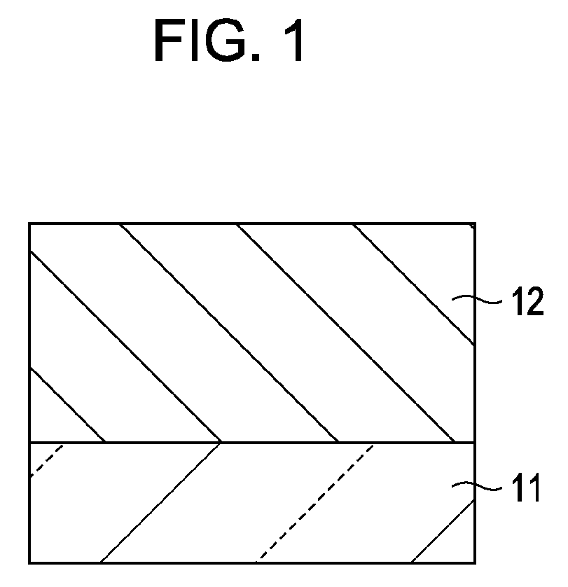
[0025]According to the embodiment of the present invention described above, by properly selecting the surface orientation of the substrate, the nitride-based III-V compound semiconductor layer having the flat surface and good crystallinity can be grown without growing the buffer layer.
[0026]Further, according to the embodiment of the present invention described above, by properly selecting the surface orientation of the substrate and properly selecting the thickness of the low-temperature GaN buffer layer, the nitride-based III-V compound semiconductor layer having the flat surface and good crystallinity can be grown just by growing the very thin low-temperature GaN buffer layer.
[0028]In addition, with the embodiment of the present invention, the nitride-based III-V compound semiconductor layer, which has the flat surface and good crystallinity and which forms the device structure of the semiconductor device, can be grown just by growing the very-thin low-temperature GaN buffer layer in advance. The semiconductor device having good characteristics can also be realized by using the nitride-based III-V compound semiconductor layer thus grown. Further, various types of electronic apparatuses, including a high-performance backlight, an illuminator, and a display, can be realized with the use of the semiconductor device having good characteristics.
Problems solved by technology
Growing the buffer layer before the growth of the nitride-based III-V compound semiconductor layer forming the device structure, as mentioned above, increases the number of steps for manufacturing a semiconductor device, and hence such a process is not desired from the viewpoint of simplifying the manufacturing steps.
Under the present situation, however, there is a difficulty in obtaining the nitride-based III-V compound semiconductor layer having a flat surface and good crystallinity by growing the nitride-based III-V compound semiconductor layer, which forms the device structure, without growing the buffer layer.
Method used
View moreImage
Smart ImageViewing Examples
Examples
first embodiment (
1. First embodiment (a method for manufacturing a semiconductor device and a semiconductor device)
second embodiment (
2. Second embodiment (method for manufacturing a light emitting diode and a light emitting diode)
third embodiment (
3. Third embodiment (a method for manufacturing a light emitting diode backlight and a semiconductor light emitting diode backlight)
Login to View More PUM
 Abstract
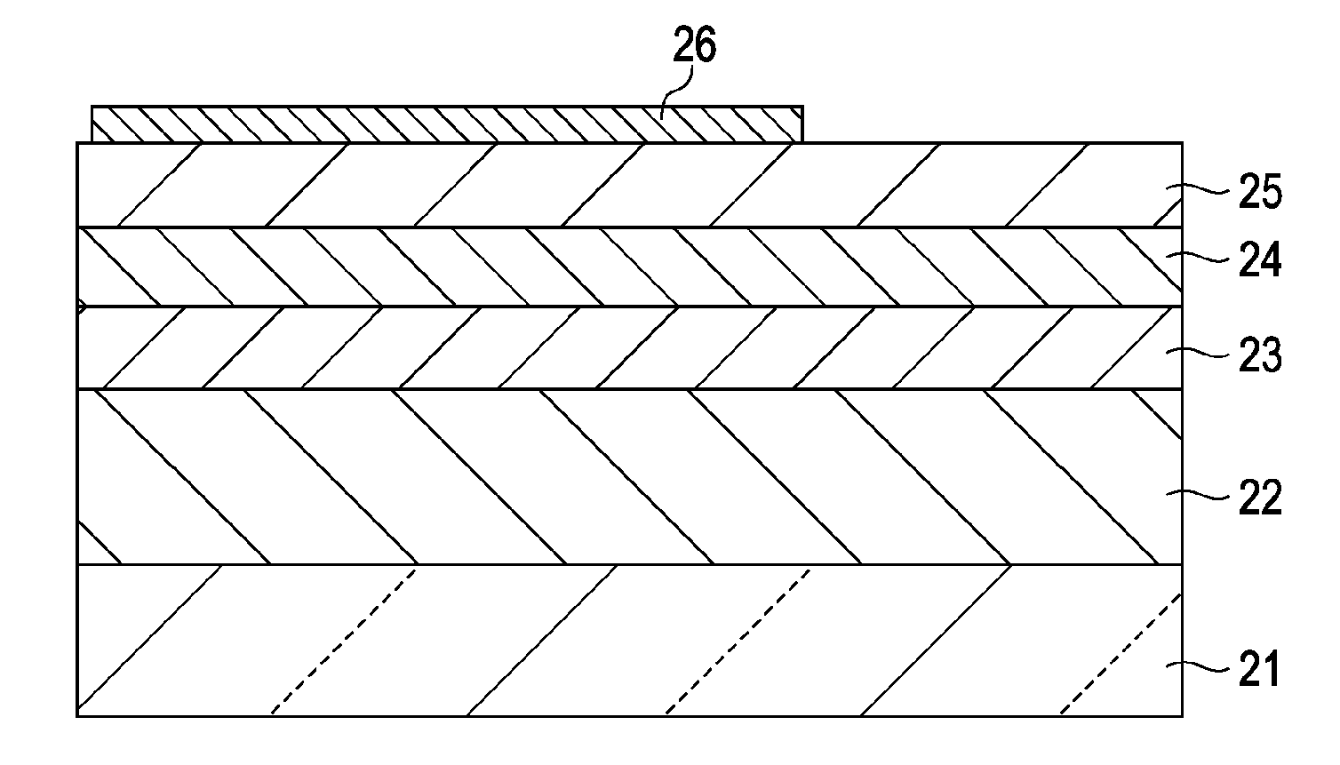
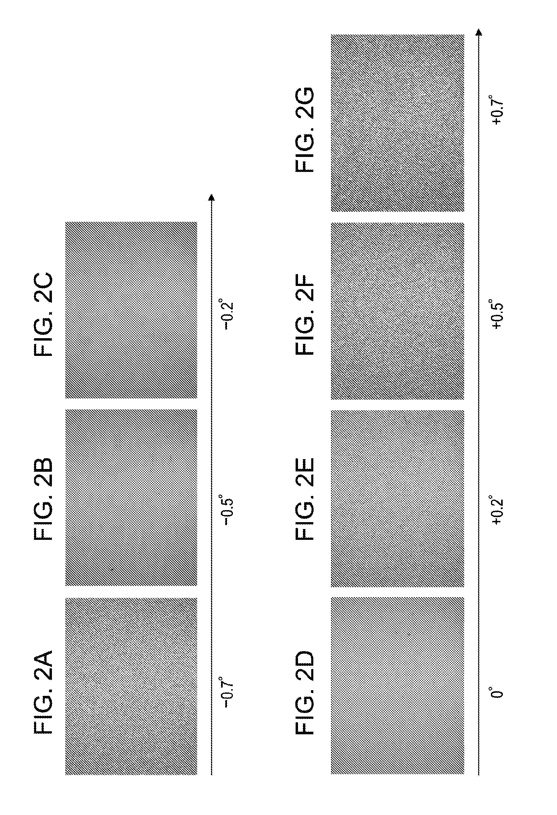
In a method for manufacturing a semiconductor device, the method includes the step of growing a nitride-based III-V compound semiconductor layer, which forms a device structure, directly on a substrate without growing a buffer layer, the substrate being made of a material with a hexagonal crystal structure and having a principal surface that is oriented off at an angle of not less than −0.5° and not more than 0° from an R-plane with respect to a direction of a C-axis.
Description
BACKGROUND OF THE INVENTION[0001]1. Field of the Invention[0002]The present invention relates to a method for manufacturing a semiconductor device and to a semiconductor device. The present invention is suitably applied to a semiconductor device, such as a light emitting diode using a nitride-based III-V compound semiconductor, for example.[0003]2. Description of the Related Art[0004]When crystal growth of a nitride-based III-V compound semiconductor, e.g., a GaN-based semiconductor, forming a device structure, is developed on a sapphire substrate, it has hitherto been general to first grow a buffer layer, which is made of GaN or AlN, on the substrate (see, for example, H. Amano et al., Appl. Phys. Lett. 48,353(1986); I. Akasaki et al., J. Cryst. Growth 98,209(1989); K. Hiramatsu et al., J. Cryst. Growth 115,628(1991); Hiroshi Amano and Isamu Akasaki, OYO BUTURI (Applied Physics) 68,768(1999); and I. Akasaki, J. Cryst. Growth 221,231(2000)). By growing a nitride-based III-V compound...
Claims
Login to View More Application Information
Patent Timeline
 IPC IPC(8): H01L29/20H01L21/20
CPCH01L33/007H01S5/3013H01L33/32H01L33/16
Inventor OHMAE, AKIRATOKUDA, KOTAARIMOCHI, MASAYUKISUZUKI, NOBUHIROSHIOMI, MICHINORIHINO, TOMONORIYANASHIMA, KATSUNORI
Owner SONY CORP


