Semiconductor integrated circuit device including a fin-type field effect transistor and method of manufacturing the same

a technology of integrated circuit device and fin-type field effect transistor, which is applied in the direction of semiconductor devices, diodes, capacitors, etc., can solve the problems of shortening the life of tddb due to fluctuations in the thickness of the insulating film of the capacitor element described above, increasing the process cost, and increasing the cost of production

Inactive Publication Date: 2013-05-21
RENESAS ELECTRONICS CORP
View PDF14 Cites 1 Cited by
  • Summary
  • Abstract
  • Description
  • Claims
  • Application Information

AI Technical Summary

Benefits of technology

The semiconductor integrated circuit device of this invention has a thicker insulating film on the upper surface of the capacitor element, which reduces electric field concentration at the edge of the lower electrode. This improvement can increase the lifespan of the insulating film.

Problems solved by technology

Therefore, introduction of a high-permittivity film (high-k film) in order to form a MIM capacitor element increases the process cost.
Therefore, when a capacitor element is formed utilizing a FinFET structure, there arises a problem that the time dependent dielectric breakdown (TDDB) life of the insulating film becomes shorter.
However, shortening of the TDDB life due to fluctuations in thickness of the insulating film of the capacitor element described above is not at all taken into consideration.
However, shortening of the TDDB life of the insulating film due to electric field concentration at the edge portion of the electrode is not at all taken into consideration.

Method used


Image

  • Semiconductor integrated circuit device including a fin-type field effect transistor and method of manufacturing the same
  • Semiconductor integrated circuit device including a fin-type field effect transistor and method of manufacturing the same
  • Semiconductor integrated circuit device including a fin-type field effect transistor and method of manufacturing the same

Examples


first embodiment

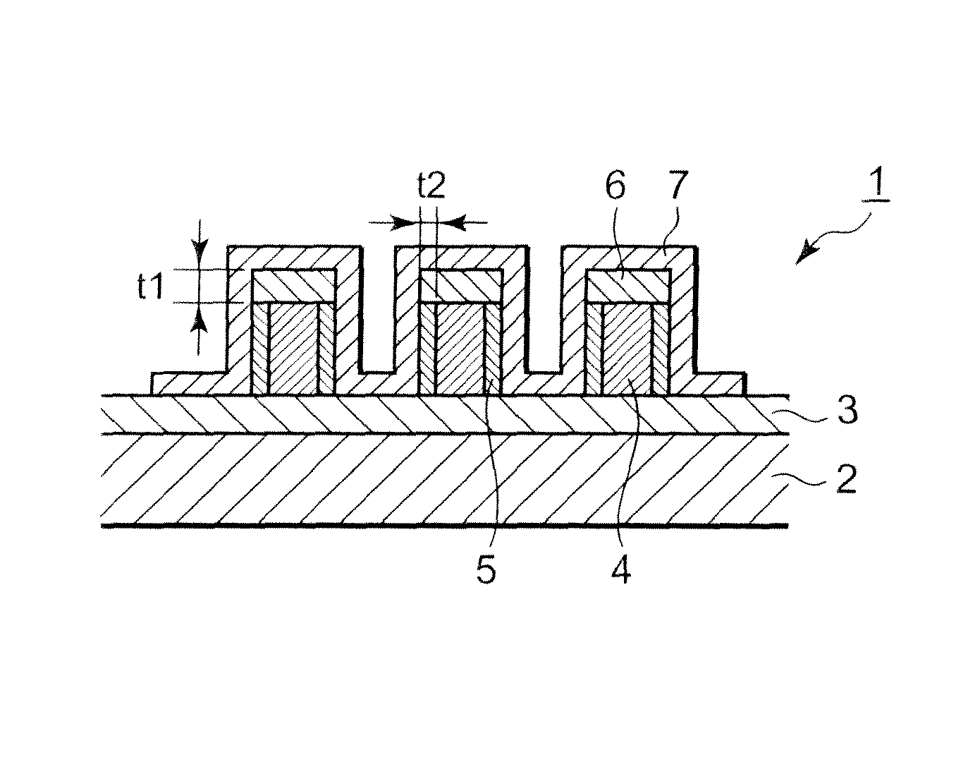
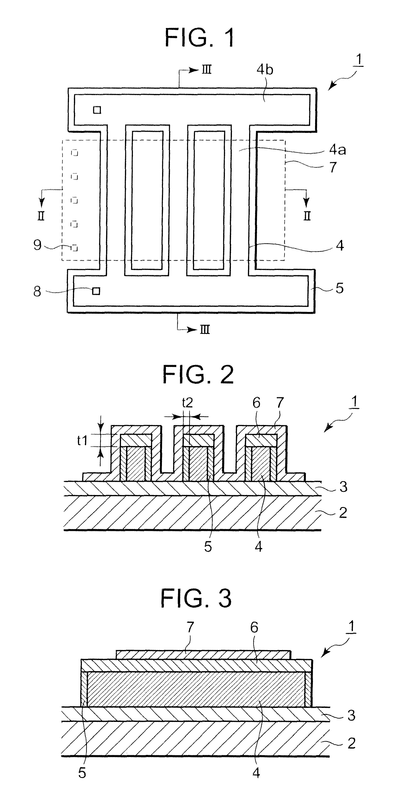
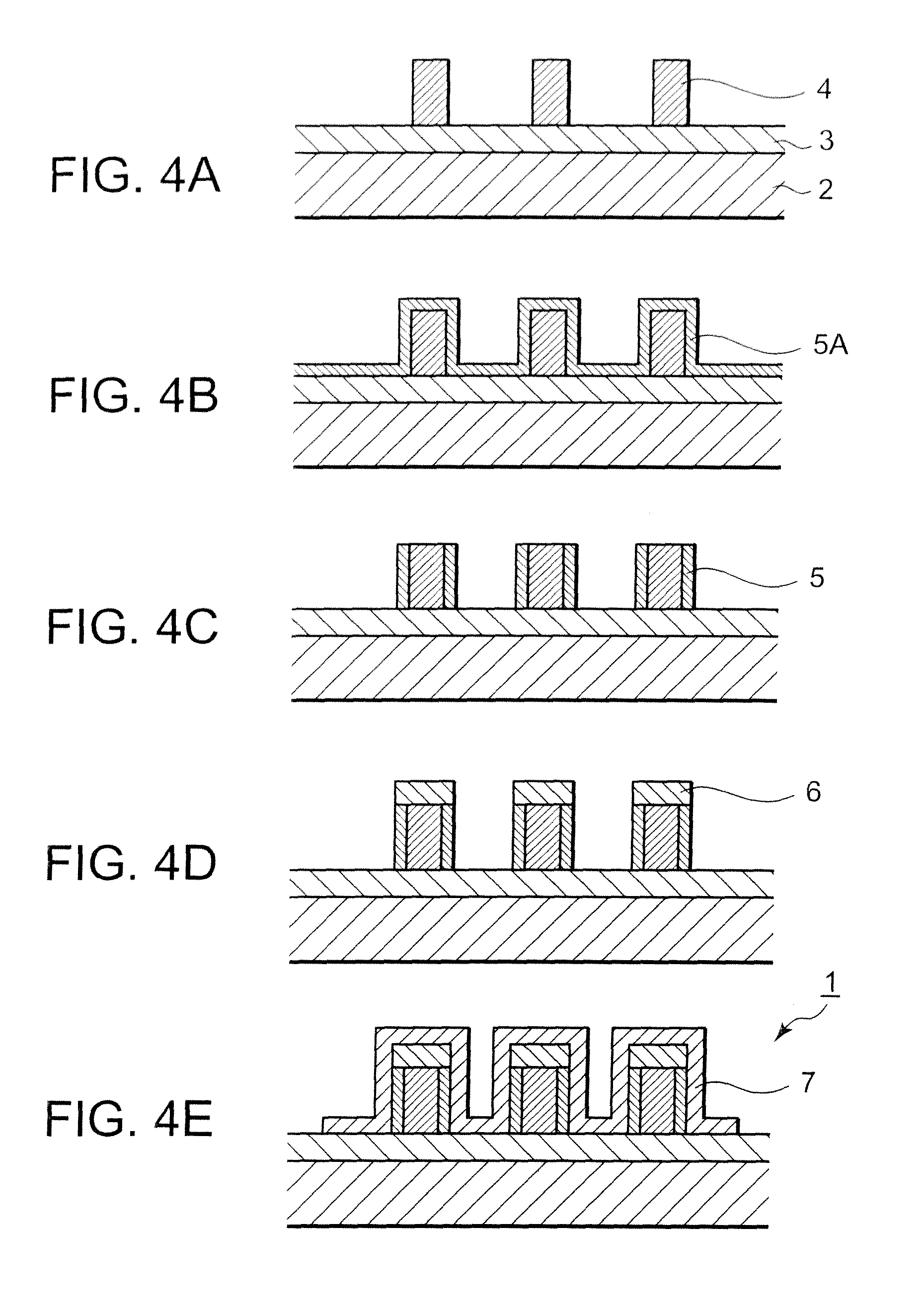
[0074]A method of forming the respective components of the capacitor elements in this embodiment is the same as the method described in the In the following, a manufacturing method is described mainly with regard to a process in which the lower electrode 4 and the upper electrode 7 of the capacitor elements are made to be of the same conductivity type (n-type).

[0075]First, impurity implantation into the lower electrode 4 of the capacitor elements is carried out in the same process as the process of impurity implantation into the semiconductor layer of the p-type FinFET (corresponding to FIG. 4A). By doing so, the lower electrode 4 and the channel region of the p-type FinFET are lightly doped and are made to be of the n-type, and the impurity concentration of the lower electrode 4 is the same as the impurity concentration of the channel region of the p-type FinFET. Further, another impurity is implanted into the semiconductor layer of the n-type FinFET to determine the concentration...

second embodiment

[0079]In the above description of the second embodiment, a case in which the lower electrode 4 and the upper electrode 7 are of the n-type is described. However, it goes without saying that the lower electrode 4 and the upper electrode 7 may be of the p-type.

[0080]Next, a semiconductor integrated circuit device according to a third embodiment of the present invention is described. FIG. 7 is a plan view of the semiconductor integrated circuit device according to the third embodiment of the present invention. FIG. 8 is a schematic sectional view taken along the line VIII-VIII of FIG. 7. In FIG. 7, an upper electrode 27 is illustrated by dotted lines and an upper surface insulating film 26 is omitted. Further, in FIGS. 7 and 8, contacts are omitted. In this embodiment, the shape of the lower electrode in plan view is different from that in the first embodiment.

[0081]In this embodiment, a lower electrode 24 is formed so as to be in a lattice shape to increase the side surface area in or...


PUM


Abstract

A semiconductor integrated circuit device, includes a first electrode including a first semiconductor layer formed on a substrate, a side surface insulating film formed on at least a part of a side surface of the first electrode, an upper surface insulating film formed on the first electrode and the side surface insulating film, a second electrode which covers the side surface insulating film and the upper surface insulating film, and a fin-type field effect transistor. The first electrode, the side surface insulating film, and the second electrode constitute a capacitor element. A thickness of the upper surface insulating film between the first electrode and the second electrode is larger than a thickness of the side surface insulating film between the first electrode and the second electrode, and the fin-type field effect transistor includes a second semiconductor layer which protrudes with respect to the plane of the substrate.

Description

[0001]The present application is a Divisional application of U.S. patent application Ser. No. 12 / 656,557, filed on Feb. 3, 2010 now abandoned, which is based on Japanese patent application No. 2009-39916, filed on Feb. 23, 2009, the entire contents of which is incorporated herein by reference.BACKGROUND OF THE INVENTION[0002]1. Field of the Invention[0003]The present invention relates to a semiconductor integrated circuit device including a capacitor element, and a method of manufacturing the same.[0004]2. Description of the Related Art[0005]In a semiconductor integrated circuit device, a capacitor element is generally used for decoupling between a power supply and GND, determining a time constant of a circuit, or other such purpose. For example, Japanese Patent Translation Publication No. 2006-503440 discloses an integrated circuit arrangement including a capacitor. The integrated circuit arrangement described in Japanese Patent Translation Publication No. 2006-503440 includes an e...

Claims


Application Information

Patent Timeline
Patent Type & Authority Patents(United States)
IPC IPC(8): H01L27/108H01L29/94
CPCH01L21/84H01L27/1203H01L28/90H01L27/0629H01L27/0805H01L29/785
Inventor FURUTA, HIROSHISHIRAI, TAKAYUKINAGA, SHUNSAKU
Owner RENESAS ELECTRONICS CORP
Why Eureka
Try Eureka