Mitigation of mask defects by pattern shifting

a pattern shifting and mask technology, applied in the field of mask defect mitigation by pattern shifting, can solve the problems of nanometer scale differences in optical path length, the inability to manufacture free of defects the complexity of photomasks used in extreme ultraviolet lithography, etc., to eliminate or minimize the impact of measured mask defects

Inactive Publication Date: 2013-06-04
GLOBALFOUNDRIES INC
View PDF9 Cites 12 Cited by
  • Summary
  • Abstract
  • Description
  • Claims
  • Application Information

AI Technical Summary

Benefits of technology

[0010]In one embodiment, the optimal pattern shift vector can be required to place all defects within the reflective region or the transparent region, or can be required to minimize the number of defects that are not placed within the reflective region or the transparent region.
[0011]According to an aspect of the present disclosure, a method for determining placement of a mask pattern with respect to a mask blank is provided. The method includes: overlaying an image of a mask pattern over an image of a mask blank annotated with a center location and at least one dimension parameter of each of measured mask defects; generating design clips centered at each of the measured defects and having a same design clip size and a same design clip shape from the image of the mask pattern; generating a binary pixel image for each of the design clips; logically compiling, pixel by pixel, the generated binary pixel images to generate a composite pixel map; and determining, from the composite pixel map, presence or absence of a pattern shift vector representing a lateral shift of the mask blank from a position at the overlaying, the lateral shift being selected to eliminate or minimize an impact of the measured mask defects during a lithographic process employing a pattern mask generated from the mask blank and including the mask pattern, wherein a computing means configured to run an automated program performs at least one of the overlaying, the generating of the design clips, the generating of the binary pixel images, the logically compiling, and the determining.
[0012]According to another aspect of the present disclosure, a method of manufacturing a patterned mask from a mask blank is provided. The method includes: overlaying an image of a mask pattern over an image of a mask blank annotated with a center location and at least one dimension parameter of each of measured mask defects; generating design clips centered at each of the measured defects and having a same design clip size and a same design clip shape from the image of the mask pattern; generating a binary pixel image for each of t

Problems solved by technology

Currently, the mask blanks used in Extreme Ultraviolet (EUV) Lithography cannot be fabricated free of defects.
However, the photomask used in Extreme Ultraviolet Lithography is much more complex, consisting of a fused silica substrate, a distributed Bragg reflector containing ˜50 alternating layers of silicon and molybdenum, a thin capping layer, and finally a patterned absorber layer.
Due to the very short wavelength of 13.6 nm employed in EUV lithography, nanometer scale differences in optical path length produce printable phase defects.
Hence, minor pits or bumps in the fused silica substrate of only a few nanometers

Method used


Image

  • Mitigation of mask defects by pattern shifting
  • Mitigation of mask defects by pattern shifting
  • Mitigation of mask defects by pattern shifting

Examples


Embodiment Construction

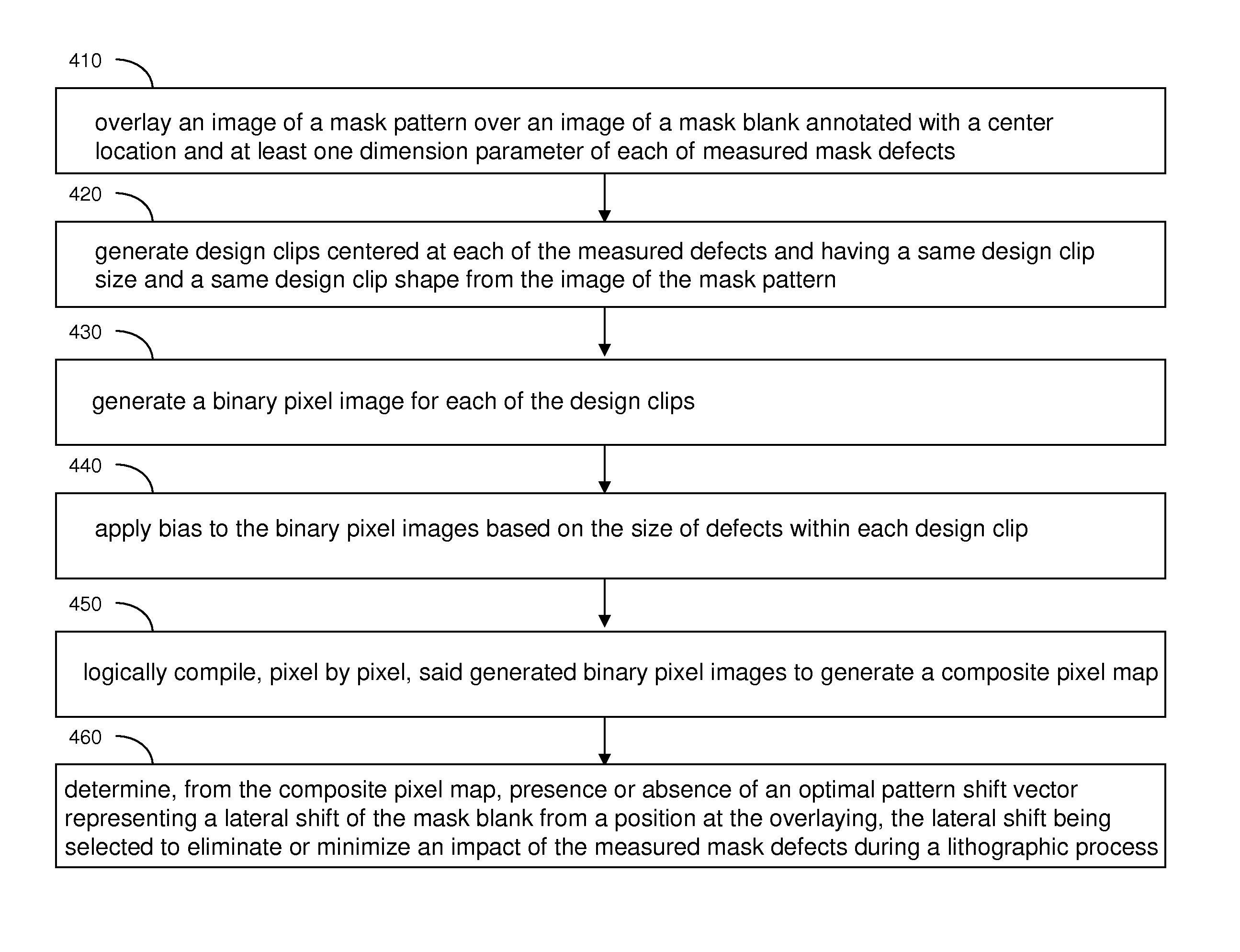
[0048]As stated above, the present disclosure relates to a methodology for a methodology for mitigating mask defects by pattern shifting and a system for implementing the same, which are now described in detail with accompanying figures. Like and corresponding elements mentioned herein and illustrated in the drawings are referred to by like reference numerals. The drawings are not necessarily drawn to scale.

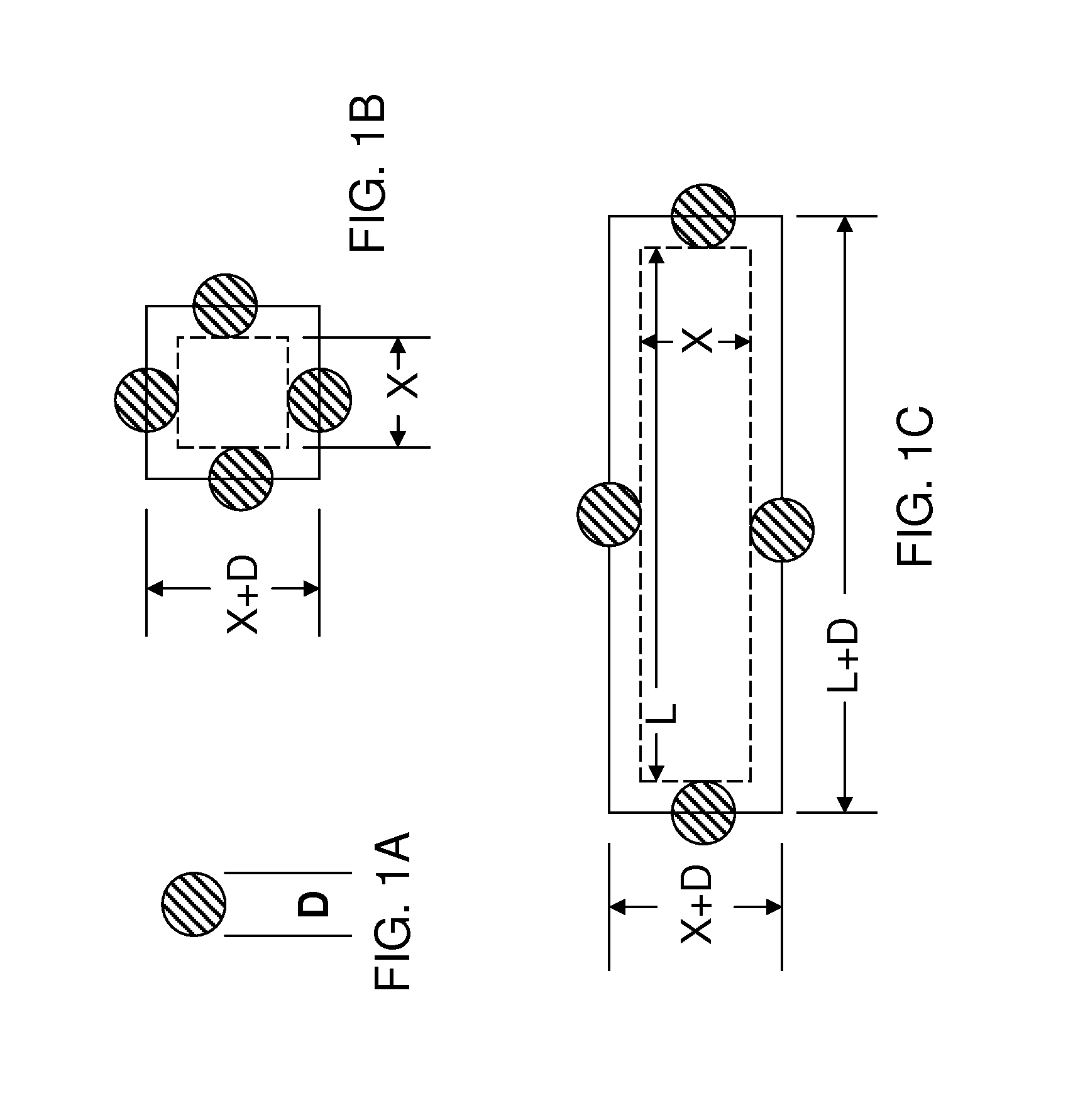
[0049]As used herein, a “design clip” refers to a subset of a design layout for a semiconductor chip that is less than the entirety of the design layout.

[0050]As used herein, a “unit grid dimension” is the unit dimension of a grid employed to design a design layout.

[0051]As used herein, a “node” of a particular dimension, e.g., 65 nm node, 45 nm node, 32 nm node, refers to a technology node employed in semiconductor industry that employs the particular dimension as a nominal dimension for lithographically printable minimum features.

[0052]As used herein, a “defect-hiding” region i...


PUM


Abstract

An image of a mask pattern is overlaid on an image of a mask blank annotated with the center location and dimensions of each measured mask defect. Design clips centered at the measured defects are generated with lateral dimensions less than allowable movement of the mask pattern over the mask blank. Each design clip is converted into a binary image including pixels corresponding to defect-activating regions and pixels corresponding to defect-hiding regions. Each pixel region representing the defect-activating region is expanded by laterally biasing peripheries by one half of the lateral extent of the defect located within the corresponding design clip. Biased design clips are logically compiled pixel by pixel to determine an optimal pattern shift vector representing the amount of pattern shift.

Description

CROSS REFERENCE TO RELATED APPLICATION[0001]This application is a continuation of U.S. patent application Ser. No. 13 / 446,369, filed Apr. 13, 2012 the entire content and disclosure of which is incorporated herein by reference.BACKGROUND[0002]The present disclosure relates to a methodology for mitigating mask defects by pattern shifting and a system for implementing the same.[0003]Currently, the mask blanks used in Extreme Ultraviolet (EUV) Lithography cannot be fabricated free of defects. A rapid method of determining the optimum placement of mask patterns on the blank to avoid these defects is described. Using this method, the probability of fabricating defect free masks when the pattern is 1) randomly placed on the mask blank, or 2) positioned optimally to avoid defects, is determined for a variety of integrated circuit designs, defect densities, and defect sizes. In addition to circular defects, oval and clusters of defects are also considered. Finally, simple analytical expressi...

Claims


Application Information

Patent Timeline
IPC IPC(8): G06F17/50
CPCG03F1/36B82Y40/00B82Y10/00G03F7/70433G03F1/24
Inventor WAGNER, ALFRED
Owner GLOBALFOUNDRIES INC
Why Eureka
Try Eureka