Bulk FinFET and SOI FinFET hybrid technology

a technology of finfet and soi fin, which is applied in the field of hybrid bulk complementary metaloxide semiconductor (cmos) fin field effect transistors, can solve the problems of difficult contacting of the body node, fast switching time and high current density of the finfet device, and increasing the difficulty of scaling with conventional doped planar devices

Inactive Publication Date: 2013-06-18
GLOBALFOUNDRIES INC
View PDF23 Cites 38 Cited by
  • Summary
  • Abstract
  • Description
  • Claims
  • Application Information

AI Technical Summary

Benefits of technology

[0005]The present invention provides hybrid bulk fin field-effect transistors (finFETs) and silicon-on-insulator (SOI) finFET devices and methods for fabrication thereof. In one aspect of the invention, a method for fabricating a complementary metal-oxide semiconductor (CMOS) circuit having a SOI finFET device and a bulk finFET device is provided. The method includes the following steps. A wafer is provided having an active layer separated from a substrate by a buried oxide (BOX), wherein the wafer has at least a first region and a second region. Portions of the active layer and the BOX are removed in the second region of the wafer so as to expose the substrate. An epitaxial material is grown in the second region of the wafer templated from the substrate. A first fin lithography hardmask is formed on the active layer in the first region of the wafer and a second fin lithography hardmask on the epitaxial material

Problems solved by technology

Continued scaling of complementary metal-oxide semiconductor (CMOS) circuits presents several technical challenges.
Scaling with conventional doped planar devices has become increasingly challenging.
Also, FinFET devices exhibit fast switching times and

Method used


Image

  • Bulk FinFET and SOI FinFET hybrid technology
  • Bulk FinFET and SOI FinFET hybrid technology
  • Bulk FinFET and SOI FinFET hybrid technology

Examples


Embodiment Construction

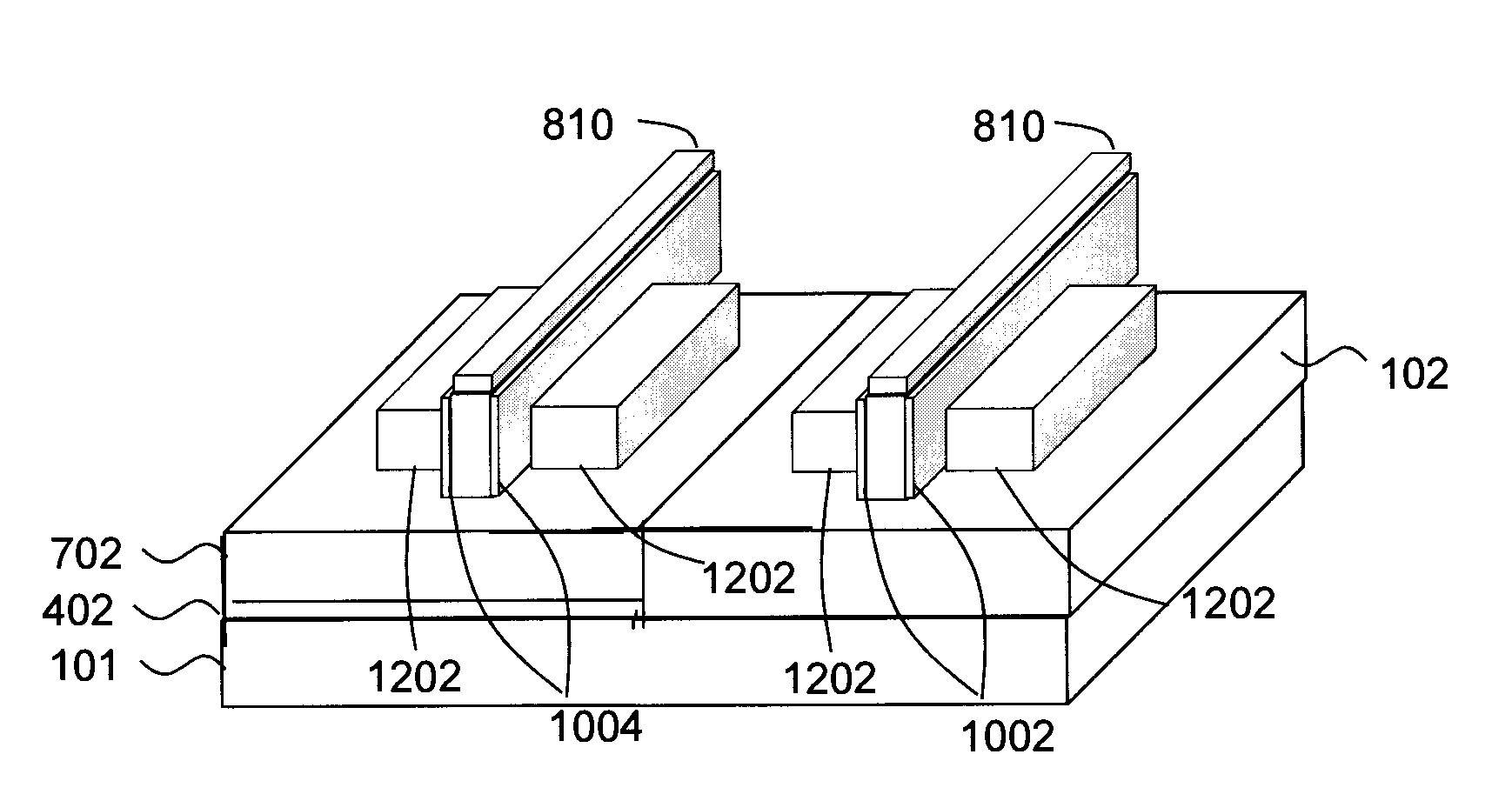
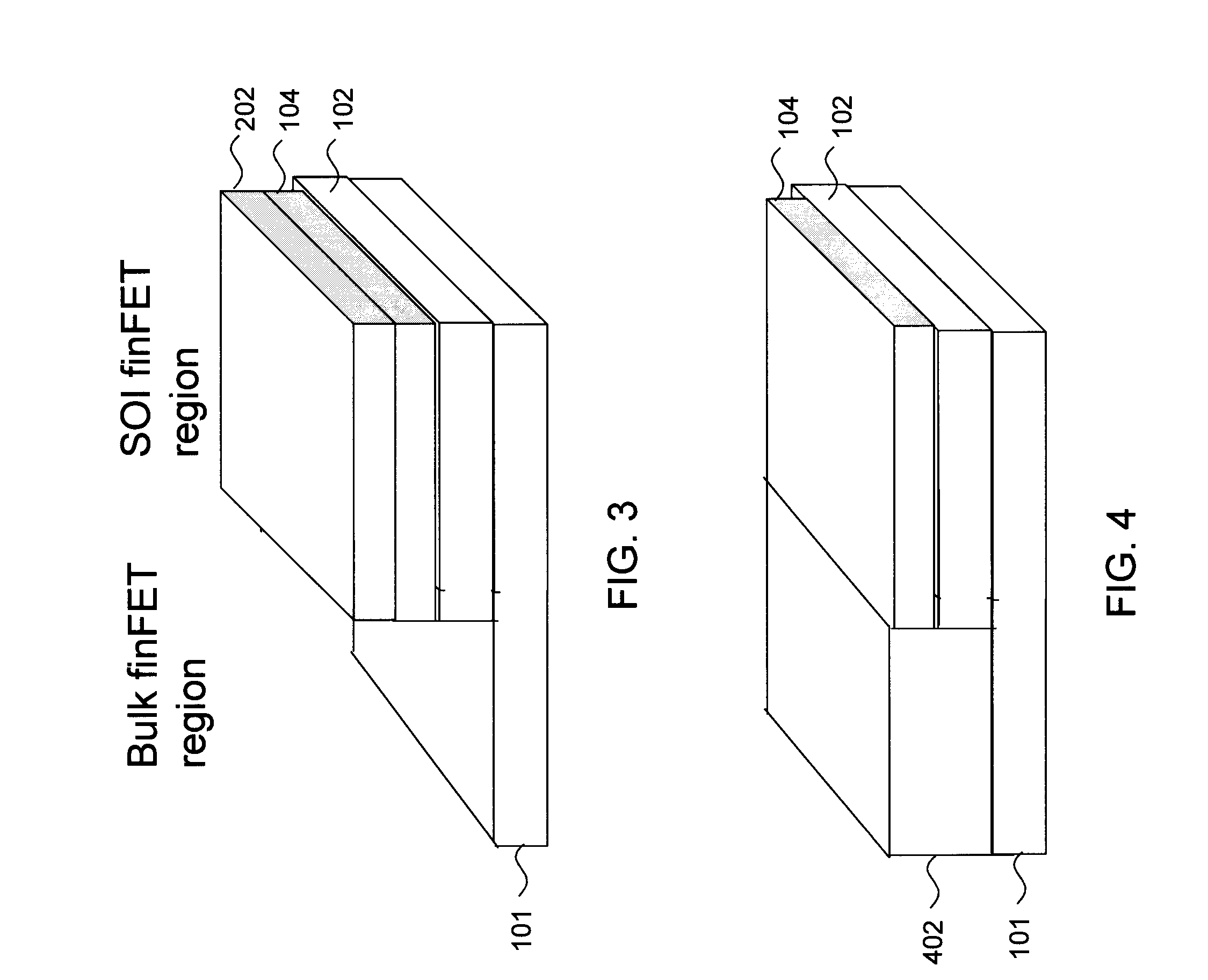
[0021]FIGS. 1-11 are diagrams illustrating an exemplary methodology for fabricating a CMOS circuit. The CMOS circuit will include a silicon-on-insulator (SOI) finFET device and a bulk finFET device both formed on the same wafer. The bulk finFETs may be used in applications where a body tie and / or good thermal tie to the substrate is preferred.

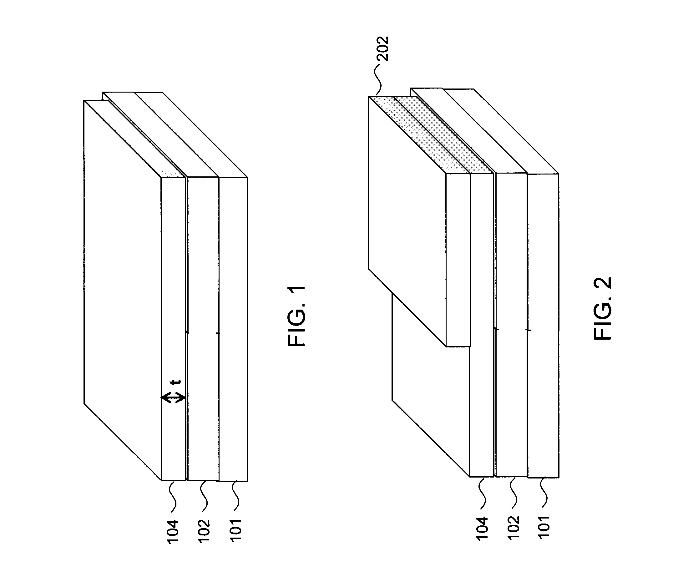
[0022]The fabrication process begins with a SOI wafer. See FIG. 1. An SOI wafer typically includes a layer of a semiconductor material (also commonly referred to as a semiconductor-on-insulator layer or SOI layer) separated from a substrate by an insulator. When the insulator is an oxide (e.g., silicon dioxide (SiO2)), it is commonly referred to as a buried oxide, or BOX. According to the present techniques, the SOI layer will serve as an active layer of the device in which the nanowires and fins will be patterned. Thus, the SOI layer will be referred to herein as an active layer.

[0023]In the example shown in FIG. 1, the starting wafer includes...


PUM


Abstract

Hybrid bulk finFET and SOI finFET devices and methods for fabrication thereof are provided. In one aspect, a method for fabricating a CMOS circuit having SOI finFET and bulk finFET devices includes the following steps. A wafer is provided having an active layer separated from a substrate by a BOX. Portions of the active layer and BOX are removed in a second region of the wafer so as to expose the substrate. An epitaxial material is grown in the second region of the wafer templated from the substrate. Fins are etched in the active layer and in the epitaxial material using fin lithography hardmasks. Gate stacks are formed covering portions of the fins which serve as channel regions of the SOI finFET/bulk finFET devices. An epitaxial material is grown on exposed portions of the fins which serves as source and drain regions of the SOI finFET/bulk finFET devices.

Description

FIELD OF THE INVENTION[0001]The present invention relates to integrated circuits, and more particularly, to hybrid bulk complementary metal-oxide semiconductor (CMOS) fin field-effect transistors (finFETs) and silicon-on-insulator (SOI) finFET devices and methods for fabrication thereof.BACKGROUND OF THE INVENTION[0002]Continued scaling of complementary metal-oxide semiconductor (CMOS) circuits presents several technical challenges. Scaling with conventional doped planar devices has become increasingly challenging. A finFET architecture offers increased scaling opportunities beyond that attainable with planar devices. See, for example, B. Yu et al., “FinFET Scaling to 10 nm Gate Length,” IEDM (2002). A finFET architecture has attractive qualities for device scaling in that no channel doping is required and also that the gate workfunction is not typically bandedge. Also, FinFET devices exhibit fast switching times and high current densities.[0003]Do to ease of fabrication, FinFETs ha...

Claims


Application Information

Patent Timeline
IPC IPC(8): H01L21/00
CPCH01L21/823821H01L21/845H01L27/1211H01L27/1207H01L27/0924
Inventor CHANG, JOSEPHINE B.CHANG, LELANDLIN, CHUNG-HSUNSLEIGHT, JEFFREY W.
Owner GLOBALFOUNDRIES INC
Why Eureka
Try Eureka