

Total reflection illuminated sensor chip, method for producing the total reflection illuminated sensor chip, and sensing method using the total reflection illuminated sensor chip
a technology of total reflection and sensor chip, which is applied in the direction of fluorescence/phosphorescence, instruments, etc., can solve the problems of not being able to stably produce sensor chips that do not, not being able to avoid the influence of (iii) above, and not being able to expend a lot of cost on the sensor chip, etc., to achieve a reduction in the amount of measuring light beam that leaks through the polishing streak, and high quantitative detection
Active Publication Date: 2013-07-02
FUJIFILM CORP
View PDF10 Cites 2 Cited by
- Summary
- Abstract
- Description
- Claims
- Application Information
AI Technical Summary
Benefits of technology
This approach enables highly quantitative detection by reducing light leakage and enhancing the electric field enhancing effect of surface plasmon, resulting in more sensitive and accurate measurements.
Problems solved by technology
However, in cases that the intended use of sensor chips is laboratory testing, it is not possible to expend much cost on the sensor chips.
In this case, it is difficult to stably produce sensor chips that do not have burrs and ridged structures (polishing streaks) formed during the molding process.
Therefore, it is difficult to avoid the influence of (iii) above.
This is because portions of measuring light beams leak through polishing streaks on surfaces on which metal films are formed (metal film formation surfaces), resulting in increased noise.
In homogenous assay systems that take advantage of the characteristic of SPFS measurement, that only signals in the vicinity of a metal film are strongly excited, and perform fluorescence detection without performing cleansing to detect the amount of a detection target substance from the variance (rate) of fluorescent signals, another factor: (v) influence of fluorescence from floating labels due to scattering of a measuring light beam; is added, and becomes a grave problem.
Method used
View moreImage
Smart ImageViewing Examples

Examples
embodiment
(Embodiment)
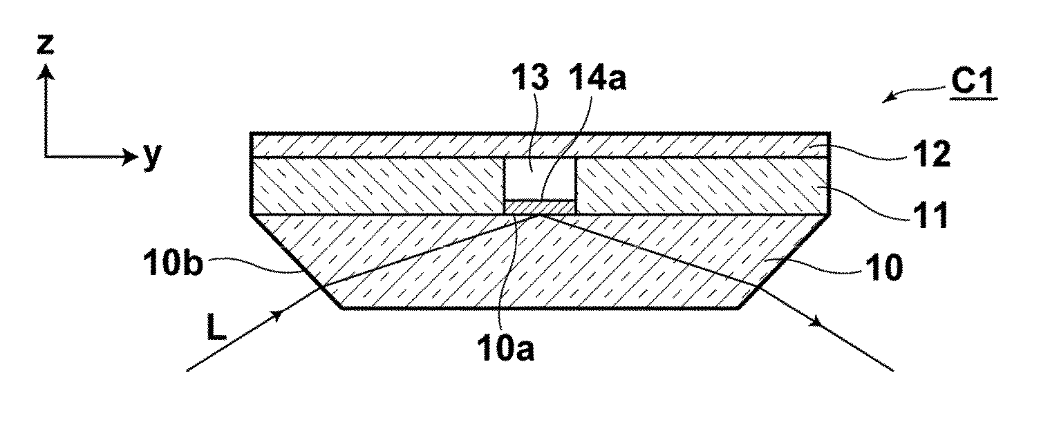
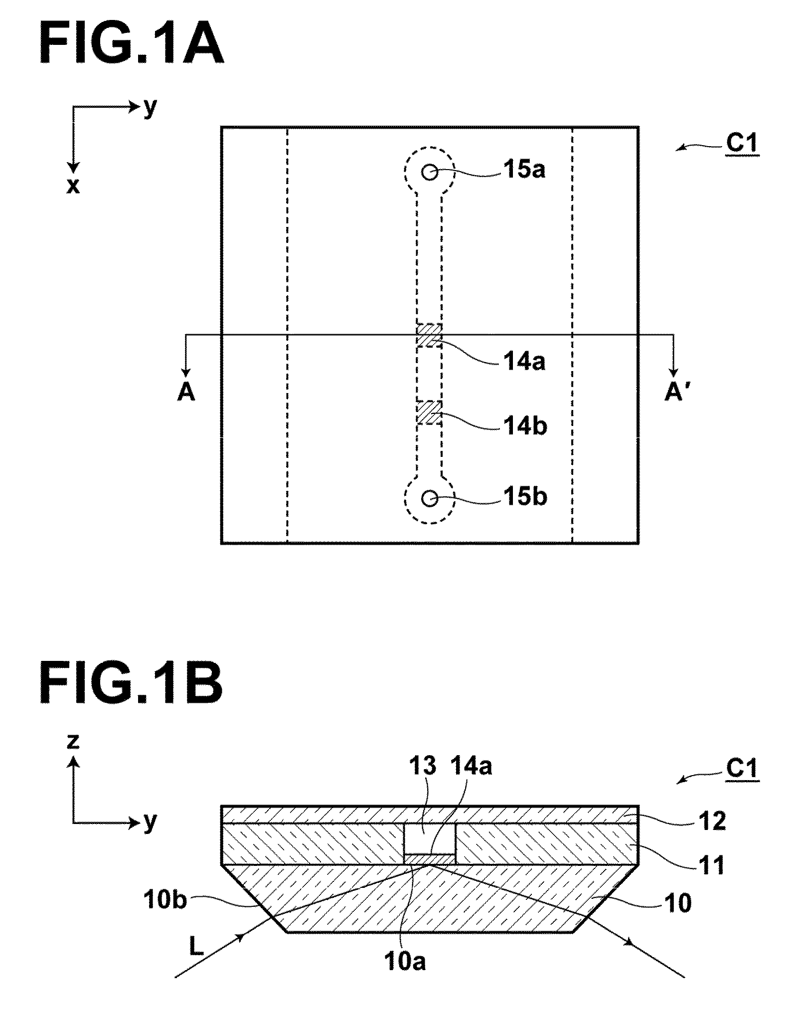
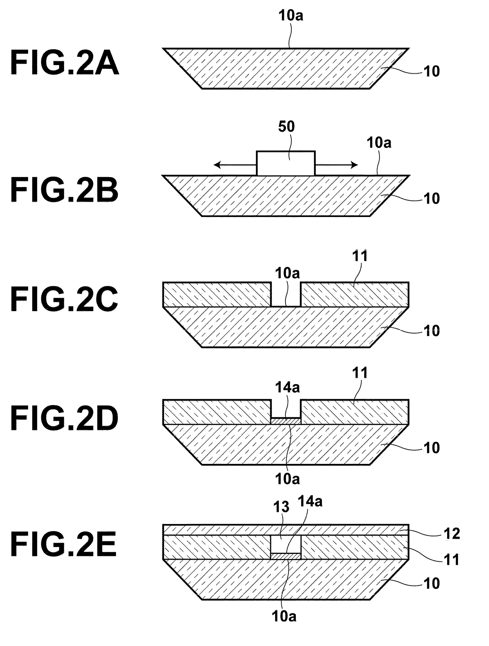
[0122]The total reflection illuminated sensor chip C2 of the second embodiment (dielectric prism: PMMA; metal film: vapor deposited Au; thickness of metal film: 50 nm; polishing streaks: directional properties in the y axis direction as illustrated in FIG. 4A) was employed to perform sensing measurements using the fluorescence detecting apparatus illustrated in FIG. 13, with hCG as an antigen (antigen concentration: 90 μM) and anti hCG as an antibody, in which cleansing was performed with PBS after secondary reactions. As a result, a ratio between signal light and noise within an entire detected signal as illustrated in FIG. 15A was obtained.
Login to View More PUM
| Property | Measurement | Unit |
|---|---|---|
| thickness | aaaaa | aaaaa |
| thickness | aaaaa | aaaaa |
| radius | aaaaa | aaaaa |
Abstract
A total reflection illuminated sensor chip is employed in a detecting method for detecting a detection target substance including the steps of: supplying a sample that includes the detection target substance onto a metal film formed on a surface of a dielectric prism, irradiating a measuring light beam onto the interface between the dielectric prism and the metal film such that conditions for total reflection are satisfied at the interface, and utilizing evanescent waves which are generated due to the irradiation of the measuring light beam to detect the detection target substance. Polishing streaks in the region of a metal film formation surface of the dielectric film, on which the metal film is formed, have directional properties with respect to a single direction.
Description
BACKGROUND OF THE INVENTION[0001]1. Field of the Invention[0002]The present invention is related to a total reflection illuminated sensor chip, which is employed in a method for detecting substances within samples by utilizing evanescent waves.[0003]2. Description of the Related Art[0004]Conventionally, detecting methods that utilize evanescent waves or surface plasmon induced by totally reflected illumination are being focused on, in biological measurements for detecting proteins, DNA, and the like. Surface plasmon are compression waves of free electrons which are generated by the free electrons vibrating as a group at the surfaces of metals. SPFS (Surface Plasmon Field enhanced fluorescence Spectroscopy) measurement is an example of a detecting method that utilizes the electric field enhancing effect of surface plasmon.[0005]SPFS measurement is a method in which detection target substances are detected, by: generating evanescent waves on a metal film that functions as a detecting ...
Claims
Login to View More Application Information
Patent Timeline
 Patent Type & AuthorityPatents(United States)
IPC IPC(8): G01N21/55G01N21/64
CPCG01N21/552G01N21/553
InventorKIMURA, TOSHIHITO
OwnerFUJIFILM CORP