Semiconductor device and display apparatus

a technology of a display device and a semiconductor, applied in the direction of semiconductor devices, electrical devices, transistors, etc., can solve the problems of increasing manufacturing costs, reducing the effect of threshold voltage variation, and no document clarifies a method for compensating or suppressing.

Active Publication Date: 2013-08-20
CANON KK
View PDF13 Cites 32 Cited by
  • Summary
  • Abstract
  • Description
  • Claims
  • Application Information

AI Technical Summary

Benefits of technology

[0008]Accordingly, in general, in the case of a conventional element using an amorphous silicon semiconductor and a device using the element, a countermeasure is not taken directly for the semiconductor channel layer, but is taken by providing a circuit for correcting the threshold voltage variation that has occurred is separated provided. This correction circuit allows the device to operate normally even when a threshold voltage variation occurs in the semiconductor. However, such correction circuit is a complicated circuit including a semiconductor element, and thus, as a result of separately providing this correction circuit, the entire circuit becomes larger in size and complicated, and the manufacturing costs are also increased. Also, if the threshold voltage variation becomes extremely large, it is difficult to correct such threshold voltage variation with the correction circuit alone.
[0030]The semiconductor device according to the present invention enables the threshold voltage of a semiconductor included in a semiconductor element to be varied so as to be close to its original state when a threshold voltage variation occurs in the semiconductor. Accordingly, the semiconductor device can normally operate all the time.
[0031]Also, use of the present invention enables suppression of or compensation for a threshold voltage variation in a semiconductor before occurrence of such threshold voltage variation, allowing the semiconductor device to operate normally.
[0032]Furthermore, the present invention enables normal operation of a semiconductor device merely by means of providing mechanisms with a simple configuration, compared to the conventional methods using a correction circuit for threshold voltage variations. Consequently, an increase in manufacturing costs can be suppressed.
[0033]Furthermore, using the present invention together with a conventional correction circuit enables normal operation of a semiconductor device even when a large threshold voltage variation beyond the correction capability of the conventional correction circuit alone occurs.
[0034]Furthermore, even when characteristics of a semiconductor element other than the threshold voltage, such as the charge mobility and / or the S value, vary together with a threshold voltage variation, the present invention enables recovery to characteristics close to those before the variation.

Problems solved by technology

However, none of the aforementioned documents clarifies a method for compensating for or suppressing a threshold voltage variation due to the aforementioned causes or a method for relatively reducing the effect of the threshold voltage variation.
However, such correction circuit is a complicated circuit including a semiconductor element, and thus, as a result of separately providing this correction circuit, the entire circuit becomes larger in size and complicated, and the manufacturing costs are also increased.
Also, if the threshold voltage variation becomes extremely large, it is difficult to correct such threshold voltage variation with the correction circuit alone.
It is desirable to keep these characteristics equal to those before the variation; however, no means has been known to enable doing so.

Method used


Image

  • Semiconductor device and display apparatus
  • Semiconductor device and display apparatus
  • Semiconductor device and display apparatus

Examples


first exemplary embodiment

(First Exemplary Embodiment)

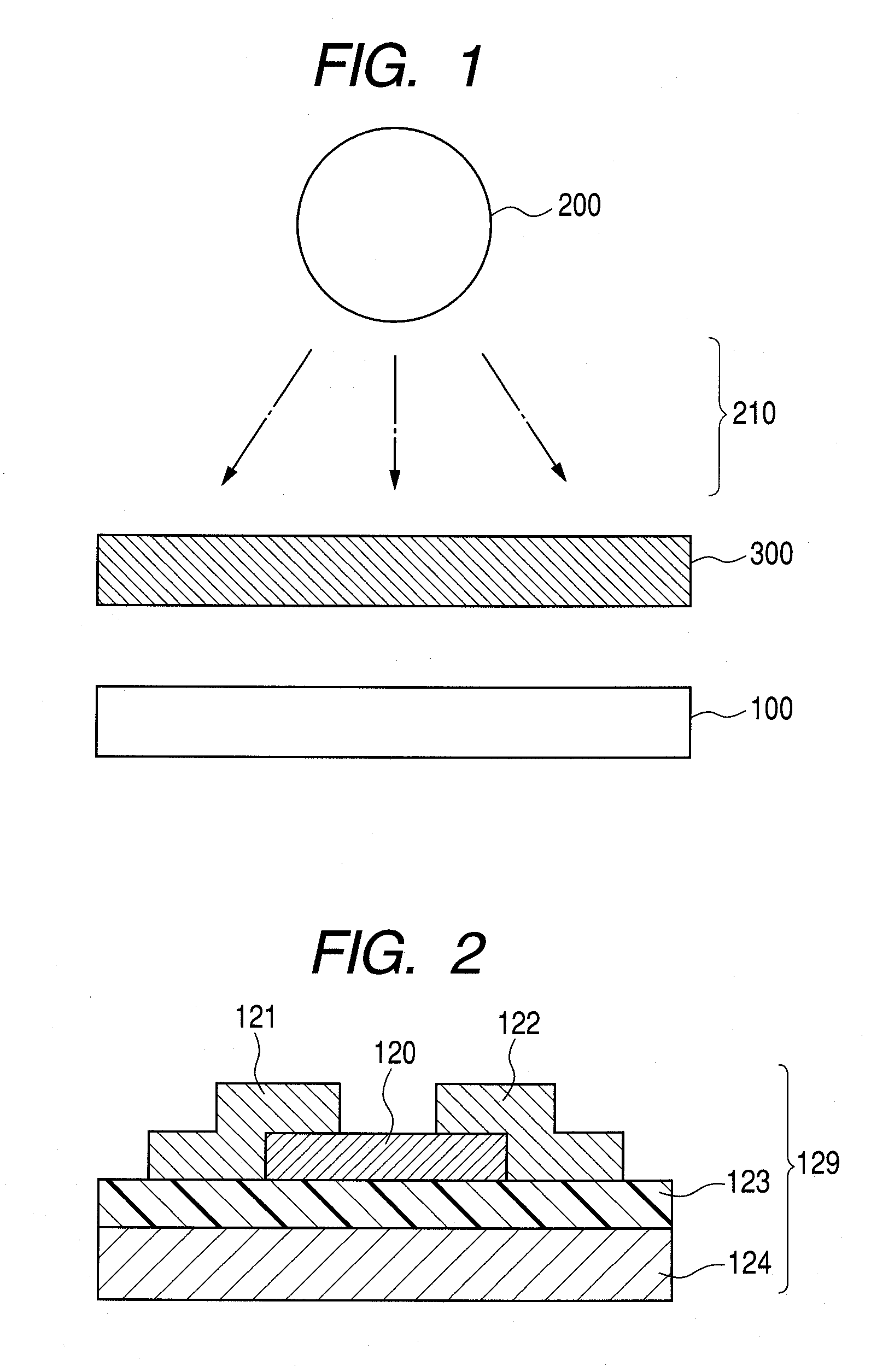
[0128]First, as a first exemplary embodiment of the semiconductor device, an exemplary embodiment of the present invention being employed in an image display apparatus, here, a liquid-crystal display (LCD) will be described below. The LCD includes a backlight light source therein. The backlight light source can be used as a light source for the present exemplary embodiment. Since most of the other display apparatuses also include a light source, the light source can be used as a light source for the present invention. For example, in the case of an organic EL display, light emitted from an organic EL layer can be used as a light source for the present invention. It should be understood that: a separate light source for the present invention may be provided, rather than using such light source; and a method of, e.g., using light from the environment as a light source may be employed. In the case of reflective display apparatuses and other apparatuses not h...

second exemplary embodiment

(Second Exemplary Embodiment)

[0136]Next, as a second exemplary embodiment of the semiconductor device, another exemplary embodiment using the present invention for a liquid-crystal display (LCD) will be described below. The present exemplary embodiment is characterized in that where the intensity of a light source included in the apparatus is excessively high for the target, scattered light is applied to the semiconductor rather than directly applying light from the light source.

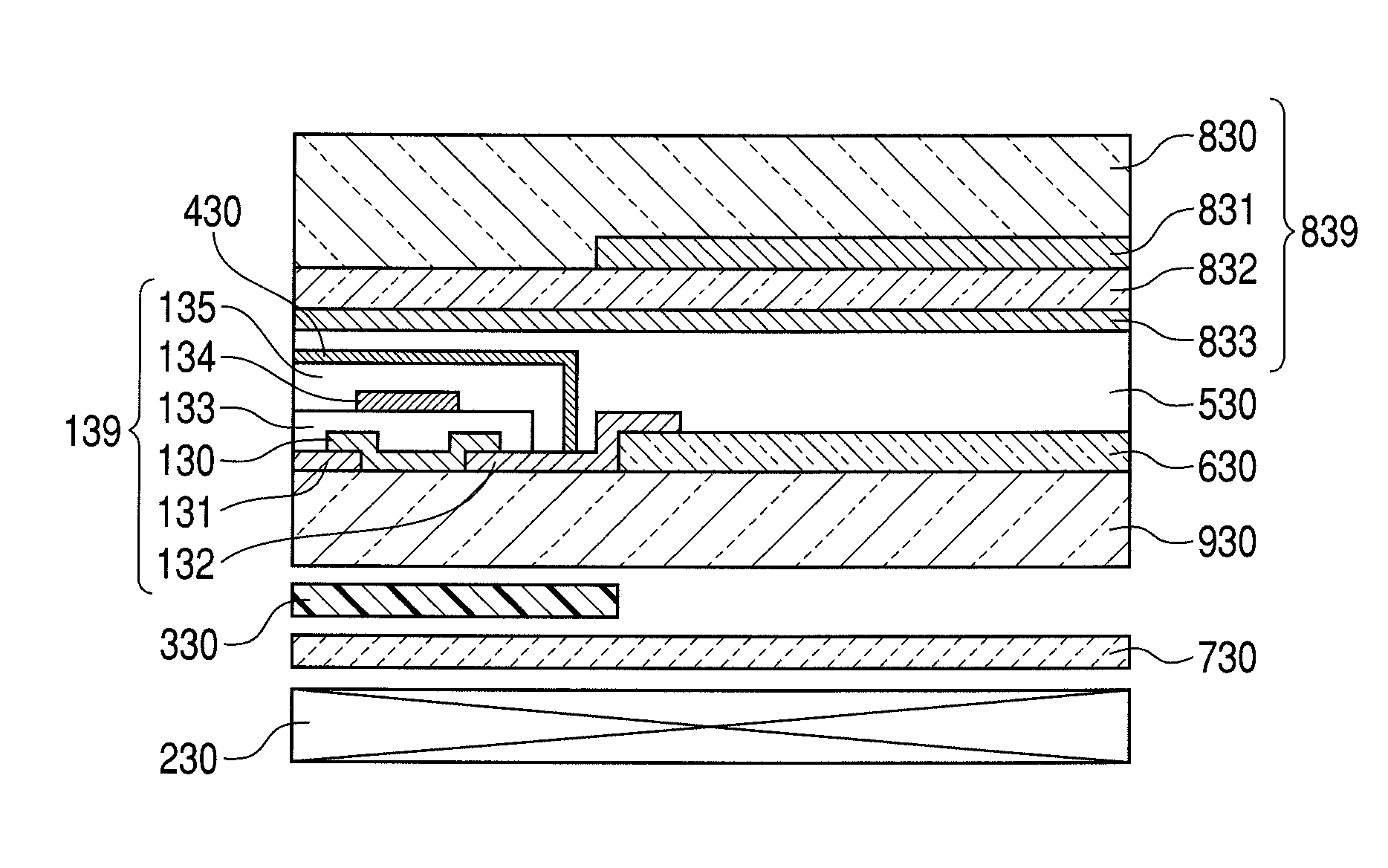
[0137]FIG. 15 illustrates a schematic structure of an LCD using the present invention. A light-blocking film 440 is formed on a glass substrate 940, and an insulating film 441 is formed over the light-blocking film 440 to fabricate a TFT 149 using an amorphous IGZO semiconductor thin film for a channel layer 140 above the part provided with the light-blocking film. One of a source 141 and a drain 142 is connected to a transparent electrode 640 provided adjacent to the TFT. A gate insulation film 143 is provi...

third exemplary embodiment

(Third Exemplary Embodiment)

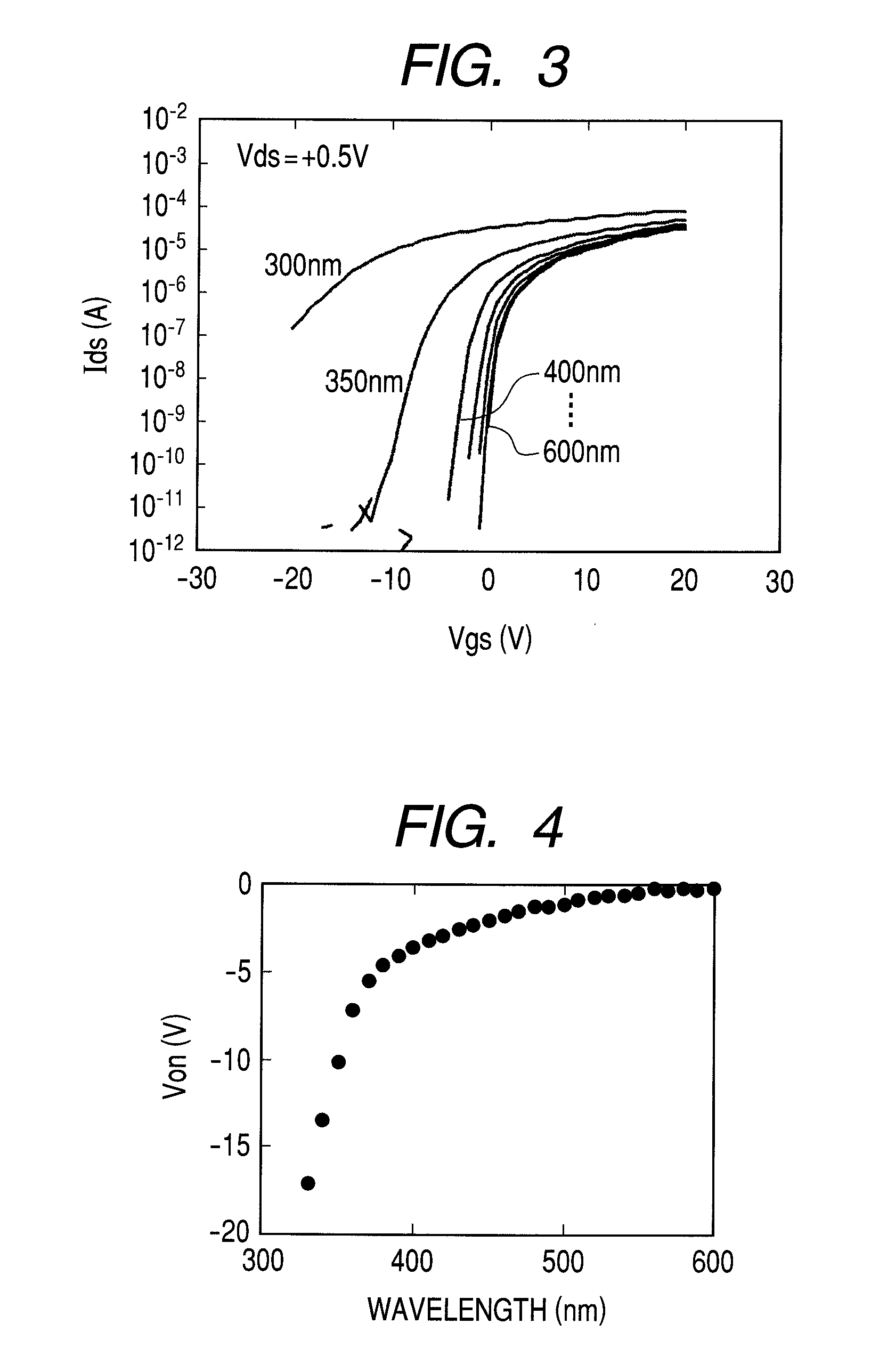
[0140]Next, as a third exemplary embodiment of the semiconductor device, a still another exemplary embodiment using the present invention for a liquid-crystal display (LCD) will be described below. In the present exemplary embodiment a characteristic variation during driving of a semiconductor element is detected while performing light irradiation with the intensity, time and wavelengths of the irradiation light varied according to the amount of the characteristic variation, enabling recovery of the characteristics of the semiconductor element to a state close to the state before the variation.

[0141]FIG. 16 illustrates a schematic structure of an LCD using the present invention. A TFT 159 using an amorphous IGZO semiconductor thin film for a channel layer 150 is fabricated on a glass substrate 950. One of a source 151 and a drain 152 is connected to a transparent electrode 650 provided adjacent to the TFT. A gate insulation film 153 is provided on the cha...


PUM


Abstract

Provided is a semiconductor device including a semiconductor element including at least a semiconductor as a component characterized by including: a mechanism for irradiating the semiconductor with light having a wavelength longer than an absorption edge wavelength of the semiconductor; and a dimming mechanism, provided in a part of an optical path through which the light passes, for adjusting at least one factor selected from an intensity, irradiation time and the wavelength of the light, wherein a threshold voltage of the semiconductor element is varied by the light adjusted by the dimming mechanism.

Description

TECHNICAL FIELD[0001]The present invention relates to a semiconductor device.BACKGROUND ART[0002]Currently, in an attempt to enhance the performance of thin-film transistors (TFTs), and lower the temperature and costs of the manufacturing process of it, a broad range of materials have been researched and studied for channel layer materials. Examples of the materials include amorphous silicon, polycrystalline silicon, microcrystalline silicon and organic semiconductors.[0003]Oxide semiconductors, which have recently been discovered, are also a prevailing group for the materials. For example, Barquinha et al., J. Non-Cryst. Sol., 352, 1756 (2006) and Yabuta et al., Appl. Phys. Lett., 89, 112123 (2006) disclose a TFT fabricating method using an amorphous In—Zn—O (IZO) thin film and an amorphous In—Ga—Zn—O (IGZO) thin film, respectively, for a channel layer.[0004]TFTs have different threshold voltages depending on the semiconductor material for the channel layer and / or the manufacturing...

Claims


Application Information

Patent Timeline
Patent Type & Authority Patents(United States)
IPC IPC(8): H01L29/72
CPCH01L29/78633H01L29/78645
Inventor YABUTA, HISATOOFUJI, MASATOTAKAI, YASUYOSHIKAWASAKI, TAKEHIKOKANEKO, NORIOHAYASHI, RYO
Owner CANON KK
Why Eureka
Try Eureka