Print processing for patterned conductor, semiconductor and dielectric materials

a technology of semiconductor and dielectric materials, applied in the field of printing, can solve the problems of difficult to achieve the ideal profile of printed features in a high-performance device such as a thin film transistor (tft), and achieve the effect of improving the profile of the resulting featur

Active Publication Date: 2013-09-10
ENSURGE MICROPOWER ASA
View PDF28 Cites 10 Cited by
  • Summary
  • Abstract
  • Description
  • Claims
  • Application Information

AI Technical Summary

Benefits of technology

[0006]The present invention concerns compositions and processes for printing relatively high performance semiconductor (e.g., silicon), conductor (e.g., metal), and dielectric (e.g., oxide) features. More specifically, the embodiments of the present invention relate to improved printing processes (e.g., inkjet printing) for forming silicon, metal and / or dielectric features, compositions useful in such printing processes, and structures formed therefrom. Controlling the solubility of the dielectric, silicon and / or metal precursor in the ink during a post-printing dynamic drying process allows for beneficial control of the profile of the resulting feature. Thus, the processes described herein allow for more precise control of critical and non-critical dimensions of dielectric, semiconductor and conductor features (e.g., lines, rectangles, T shapes, L shapes, H shapes, dumbbell shapes, tabs, circles, squares, combinations thereof, etc.) in printed electronic circuits and devices.
[0008]Ink viscosity can also substantially affect the pinning and profile of the structure or film formed from the printed ink. A solute that increases the viscosity of the ink as the ink dries may increase the probability and / or reproducibility of obtaining a dome-shaped profile, as opposed to a “coffee-ring” type profile. In many applications, a dome-shaped profile (particularly in a cross section taken along a relatively short axis in a layout view) may be an ideal profile for use in printed dielectric, semiconductor and conductor applications. In many inks, viscosity may be increased by higher molecular weight (MW) solutes in the ink, for instance a polysilane or other Group IVA compound (e.g., a compound comprising Si and / or Ge) having at least 15 Si and / or Ge atoms, nanoparticles of silicon, germanium, metal, metal oxide and / or nitride, etc. An increased viscosity tends to offset (or reduce the rate of) mass transport to the edge of the pinning site, and may result in a dome-shaped profile that can be maintained during evaporation of the solvent.
[0009]Embodiments of the present invention provide improved printing process conditions that allow for more precise control of a cross-sectional profile and / or dimensions of a dielectric, semiconductor or conductor feature, such as a line, rectangle, T shape, L shape, H shape, dumbbell shape, tab, circle, square, combination thereof, etc. The method of printing a feature on a substrate (e.g., printing a liquid semiconductor-containing composition to form a line or other shape) with improved pinning and more precisely controlled dimensions may include the steps of: (a) printing an ink comprising a precursor of a material in a pattern on a substrate, (b) precipitating the precursor (or a higher molecular weight or more insoluble derivative thereof) in the pattern to form a pinning line, (c) substantially evaporating the solvent to form the feature defined by the pinning line and comprising the precursor (or a higher molecular weight or more insoluble derivative thereof), and (d) converting the precursor (or a higher molecular weight or more insoluble derivative thereof) to the patterned material. The method may further comprise controlling a contact angle of the ink by depositing a surface energy modifying agent on said substrate before printing the precursor ink, and converting the precursor (or a higher molecular weight or more insoluble derivative thereof) may comprise curing the precursor (or derivative thereof and / or material).

Problems solved by technology

Previously, there have been challenges in precisely controlling certain critical dimensions in printed electrically functional features (and especially high resolution dielectric, conductor and semiconductor features).
Conventional printing process conditions have resulted in poor control of length, height (thickness), cross-sectional profile and width of printed lines and islands.
Thus, an ideal profile for printed features in a high performance device such as a thin film transistor (TFT) has been difficult to achieve.
However, substrates typically used in manufacturing electronic devices are generally non-absorbing.

Method used


Image

  • Print processing for patterned conductor, semiconductor and dielectric materials
  • Print processing for patterned conductor, semiconductor and dielectric materials
  • Print processing for patterned conductor, semiconductor and dielectric materials

Examples


Embodiment Construction

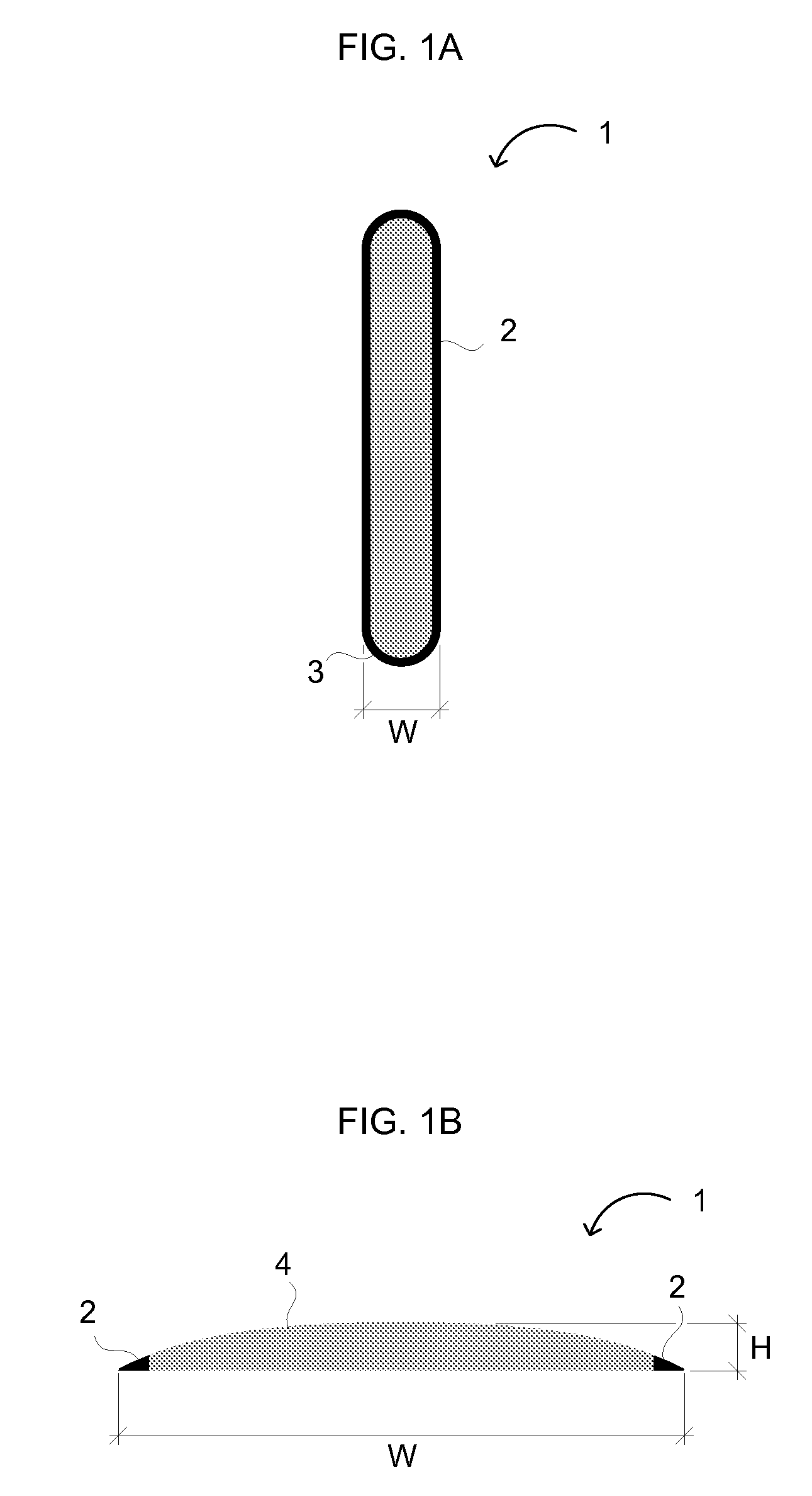
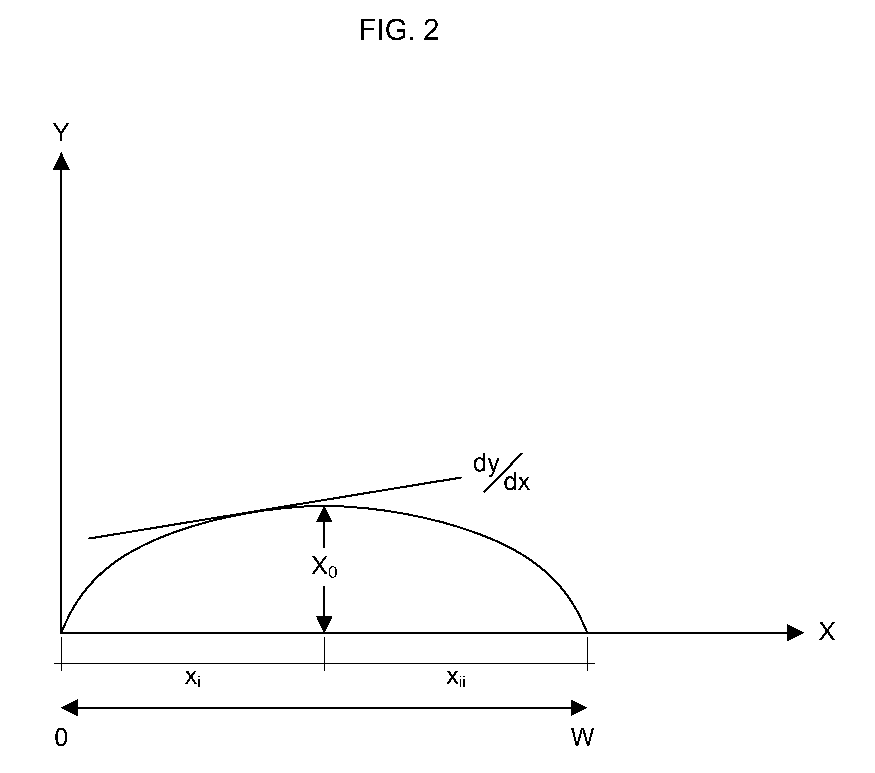
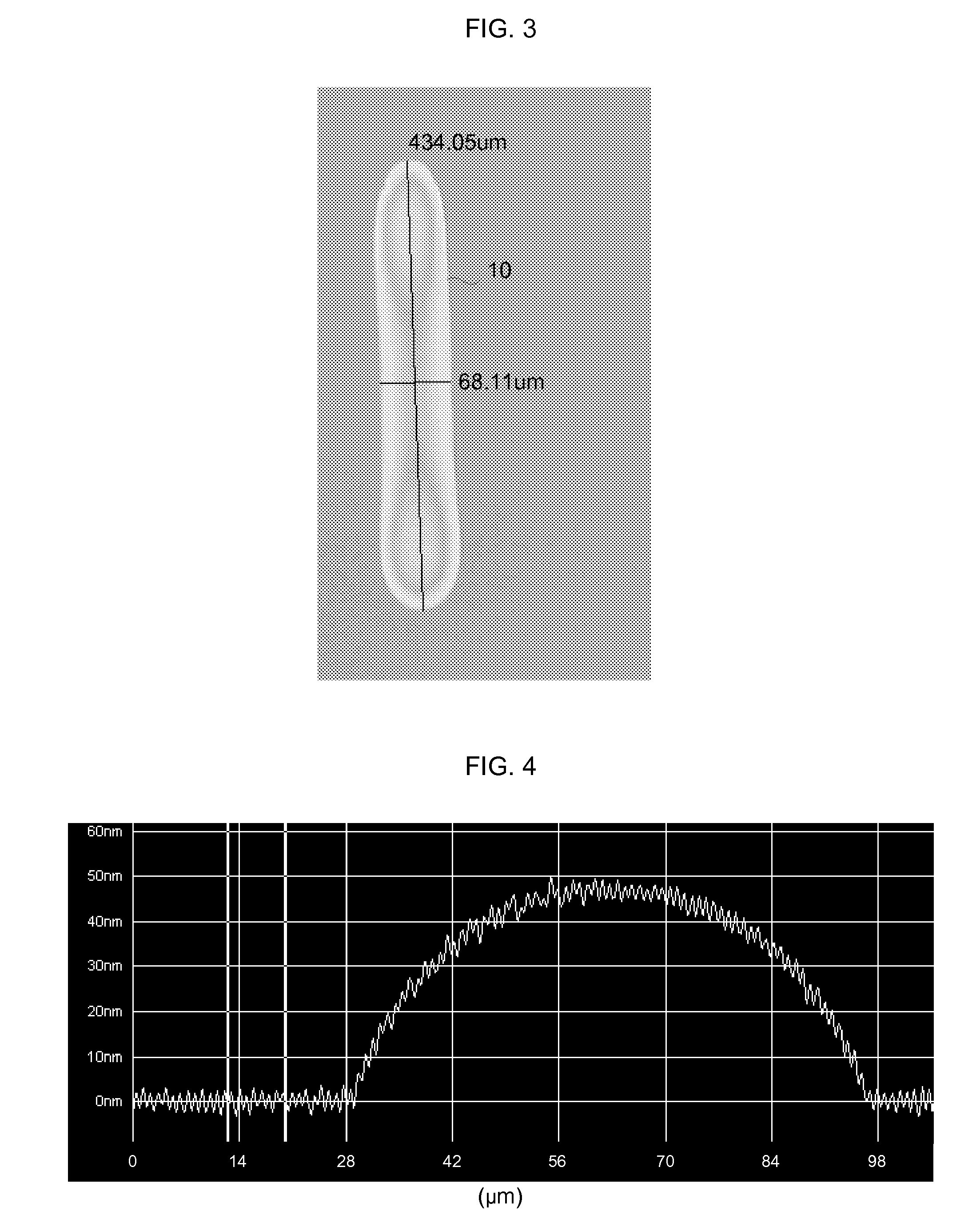
[0020]Reference will now be made in detail to preferred embodiments of the invention, examples of which are illustrated in the accompanying drawings. While the invention will be described in conjunction with the preferred embodiments, it will be understood that they are not intended to limit the invention to these embodiments. On the contrary, the invention is intended to cover alternatives, modifications and equivalents that may be included within the spirit and scope of the invention as defined by the appended claims. Furthermore, in the following disclosure, numerous specific details are given to provide a thorough understanding of the invention. However, it will be apparent to one skilled in the art that the present invention may be practiced without these specific details. In other instances, well-known methods, procedures, components, and circuits have not been described in detail, to avoid unnecessarily obscuring aspects of the present invention.

[0021]In the present disclosur...


PUM

PropertyMeasurementUnit
viscosityaaaaaaaaaa
viscosityaaaaaaaaaa
wavelengthaaaaaaaaaa

Abstract

Embodiments relate to printing features from an ink containing a material precursor. In some embodiments, the material includes an electrically active material, such as a semiconductor, a metal, or a combination thereof. In another embodiment, the material includes a dielectric. The embodiments provide improved printing process conditions that allow for more precise control of the shape, profile and dimensions of a printed line or other feature. The composition(s) and / or method(s) improve control of pinning by increasing the viscosity and mass loading of components in the ink. An exemplary method thus includes printing an ink comprising a material precursor and a solvent in a pattern on the substrate; precipitating the precursor in the pattern to form a pinning line; substantially evaporating the solvent to form a feature of the material precursor defined by the pinning line; and converting the material precursor to the patterned material.

Description

RELATED APPLICATIONS[0001]This application claims the benefit of U.S. Provisional Patent Application Nos. 60 / 927,984 and 60 / 997,335, respectively filed May 4, 2007 and Oct. 1, 2007, incorporated herein by reference in its entirety.FIELD OF THE INVENTION[0002]Embodiments of the present invention relate to printing (e.g., inkjet printing) a composition containing precursors to silicon, germanium, metal and / or dielectrics to form semiconductor, conductor and / or dielectric features. The embodiments provide improved printing process conditions that allow for more precise control of a critical dimension of a dielectric, conductor or semiconductor feature. In one embodiment, to print a semiconductor film in a predetermined shape (e.g., an anisotropic shape, such as a line or an island), the printed silicon-containing ink may be fixed or “pinned.” This and other embodiments described below provide processes that may improve control of feature pinning and the resulting film profile. As a res...

Claims


Application Information

Patent Timeline
Patent Type & Authority Patents(United States)
IPC IPC(8): H01L29/16C08F2/42C08J3/28
CPCC09D11/101C09D11/322C09D11/36C09D11/54H01L21/02532H01L21/02601H01L21/28008H01L29/6675H01L29/78696C09D5/24H01B3/02H01L21/02628Y10T428/24802H01L27/1292B82Y40/00H01L21/20
Inventor SCHER, ERIKMOLESA, STEVENROCKENBERGER, JOERGKAMATH, ARVINDMORI, IKUO
Owner ENSURGE MICROPOWER ASA
Why Eureka
Try Eureka