Read sensing circuit and method with equalization timing
- Summary
- Abstract
- Description
- Claims
- Application Information
AI Technical Summary
Benefits of technology
Problems solved by technology
Method used
Image
Examples
Embodiment Construction
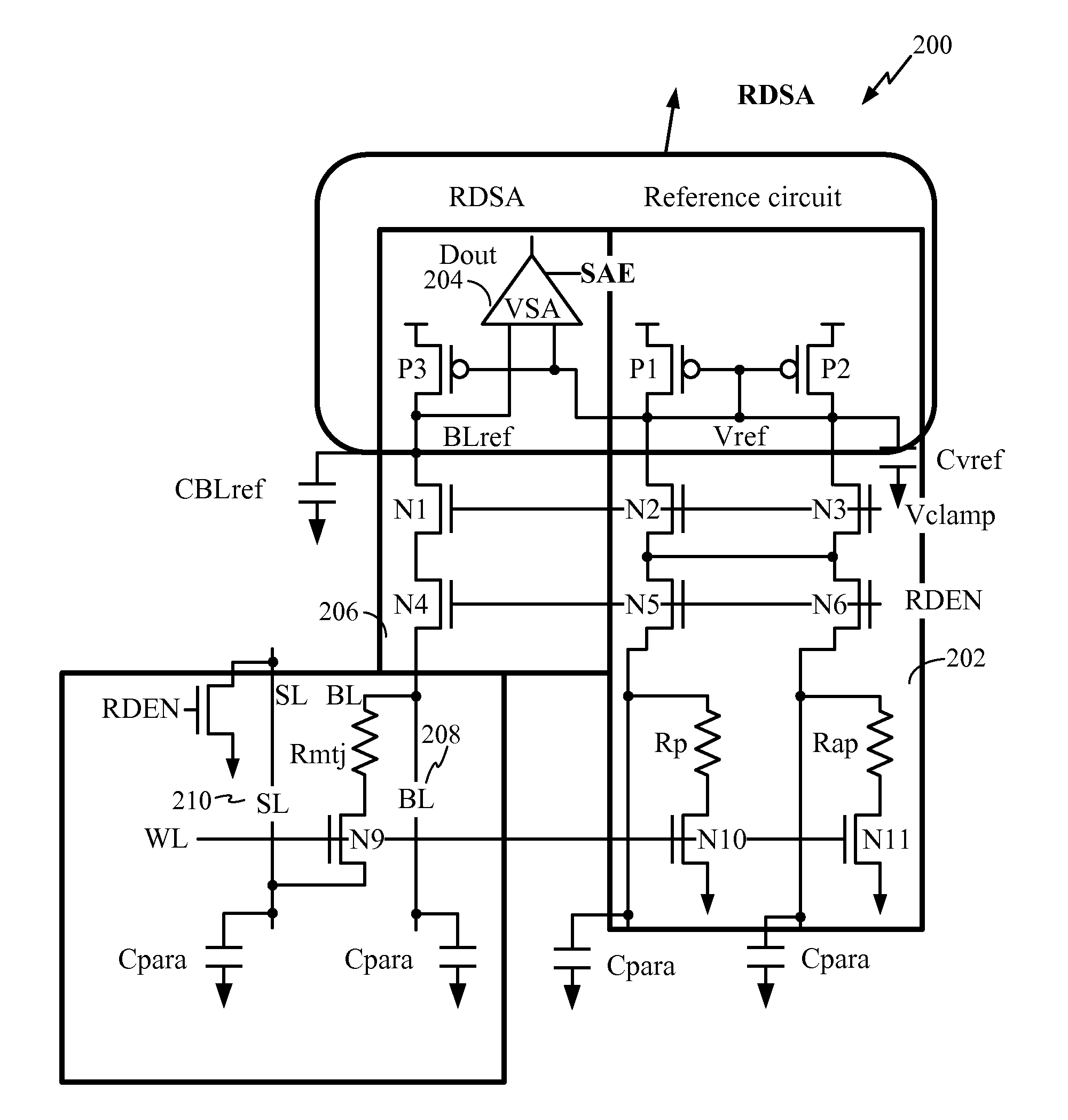
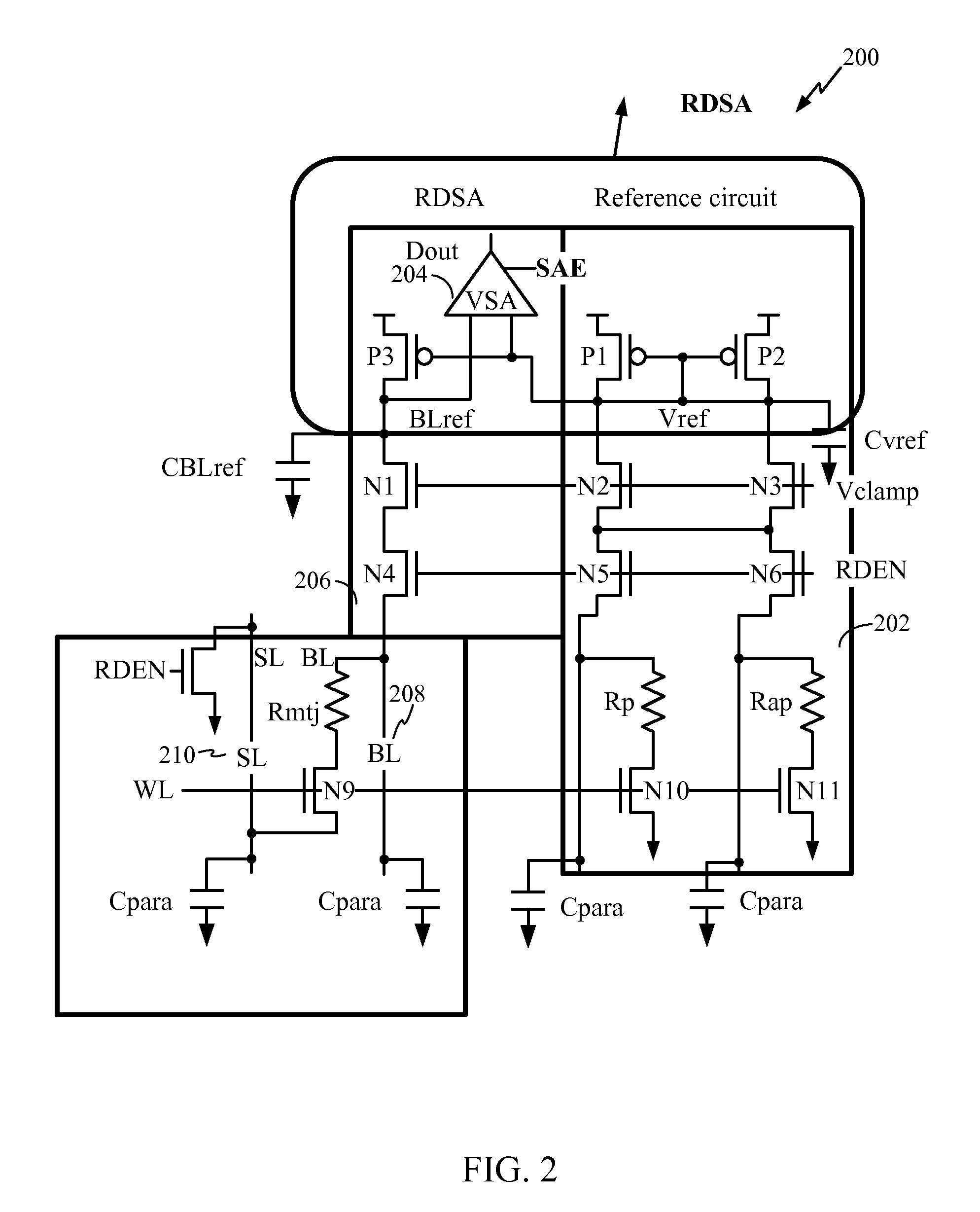
[0023]A read sensing circuit for an MRAM cell is described with reference to FIG. 2 in which a reference circuit generates a reference voltage to be compared with an output voltage from a data circuit including a memory cell array in a voltage sense amplifier (VSA). A read sensing circuit 200 includes a reference circuit portion 202 for generating the reference voltage level at node Vref for comparing with a bit line voltage level at node BLref (output) of a memory array 206. Node Vref and node BLref are coupled to a voltage sense amplifier 204 that compares signal levels on node Vref and node BLref to determine a state of an MTJ memory element Rmtj in the memory array 206. Although a single bit cell with an MTJ is shown, the memory array 206 includes numerous bit cells that will store data. The reference circuit portion 202 includes a first current path through a first reference MTJ (Rp) that is fixed in a parallel low resistance state, and a second current path through a second re...
PUM
 Abstract
Description
Claims
Application Information


