Constraint optimization of sub-net level routing in asic design

a technology of constraint optimization and routing, applied in the field of optimizing connection constraints in integrated circuit design, can solve the problems of chip failure to operate reliably (e.g., execute logic operations as intended), chip failure to meet the requirements of the design,

Active Publication Date: 2013-09-24
GLOBALFOUNDRIES US INC
View PDF8 Cites 91 Cited by
  • Summary
  • Abstract
  • Description
  • Claims
  • Application Information

AI Technical Summary

Benefits of technology

[0012]Various embodiments for optimizing connection constraints in an integrated circuit (IC) design are disclosed. In some embodiments, a target timing path associated with a first of a plurality of sub-connections of the integrated circuit is determined. The first of the plurality of sub-connections is associated with a current connection constraint set. A timing probability value associated with the first of the plurality of sub-connections is determined based, at least in part, on the target timing path associated with the first of the plurality of sub-connections. The timing probability value indicates a probability that timing closure is satisfied on the target timing path associated with the first of the plurality of sub-connections. A route probability value associated with the first of the plurality of sub-connections is determined based, at least in part, on the target timing path associated with the first of the plurality of sub-connections. The route probability value indicates a probability that a physical routing track on the target timing path associated with the first of the plurality of sub-connections resolves congestion. A connection constraint model to which the first of the plurality of sub-connections corresponds is identified based, at least in part, on the timing probability value associated with the first of the plurality of sub-connections and the route probability value associated with the first of the plurality of sub-connections. The current connection constraint associated with the first of the plurality of sub-connections is modified in accordance with the connection constraint model to which the first of the plurality of sub-connections corresponds.
[0012]Various embodiments for optimizing connection constraints in an integrated circuit (IC) design are disclosed. In some embodiments, a target timing path associated with a first of a plurality of sub-connections of the integrated circuit is determined. The first of the plurality of sub-connections is associated with a current connection constraint set. A timing probability value associated with the first of the plurality of sub-connections is determined based, at least in part, on the target timing path associated with the first of the plurality of sub-connections. The timing probability value indicates a probability that timing closure is satisfied on the target timing path associated with the first of the plurality of sub-connections. A route probability value associated with the first of the plurality of sub-connections is determined based, at least in part, on the target timing path associated with the first of the plurality of sub-connections. The route probability value indicates a probability that a physical routing track on the target timing path associated with the first of the plurality of sub-connections resolves congestion. A connection constraint model to which the first of the plurality of sub-connections corresponds is identified based, at least in part, on the timing probability value associated with the first of the plurality of sub-connections and the route probability value associated with the first of the plurality of sub-connections. The current connection constraint associated with the first of the plurality of sub-connections is modified in accordance with the connection constraint model to which the first of the plurality of sub-connections corresponds.

Problems solved by technology

It is noted that if the predetermined timing requirements cannot be satisfied, the chips may not operate reliably (e.g., execute their logic operations as intended) at a predetermined temperature and voltage.
It is noted that if the design rule checks are not satisfied, short circuits, open circuit, and other such connection errors can occur in the chips, causing malfunctioning (or unreliable operation) of the chips.
Thus, the optimization processes to ensure timing closure result in a decrease in the amount of available wiring resources, additional problems because of the added metal wires and metal vias, and an increase in the amount of time to further optimize the wiring resources.
However, the changes made to the metal layers and metal vias may directly affect (e.g., increase or decrease) the length of the original metal wires.
This can result in a variation in the parameters (e.g., resistance and capacitance) of the metal wires, which in turn can result in a variation in the signal transmission time and in the delay.
These changes (e.g., an increase or a decrease in the signal transmission time, the delay, etc.) can affect the timing closure, especially in the regions of the chip where the wiring resources are limited and where it is difficult to change the metal layers and metal vias.
In the regions of the chip that are associated with limited wiring resources, a slight change in one part of the region can affect the entire design of the chip.
This may increase the length of the original metal wire and may even result in additional metal layers and metal vias.
This increase a can further affect the parameters (e.g., resistance and capacitance) of the metal wires which, in turn, can result in a variation in signal transmission time and delay.
Thus, the process for ensuring physical closure, especially in the regions where the wiring resources are limited, can result in a variation of the signal transmission time and the delay on the wire which, in turn, can influence the timing closure.
However, it can be difficult for existing electronic design tools to balance the two constraints.

Method used


Image

  • Constraint optimization of sub-net level routing in asic design
  • Constraint optimization of sub-net level routing in asic design
  • Constraint optimization of sub-net level routing in asic design

Examples


Embodiment Construction

)

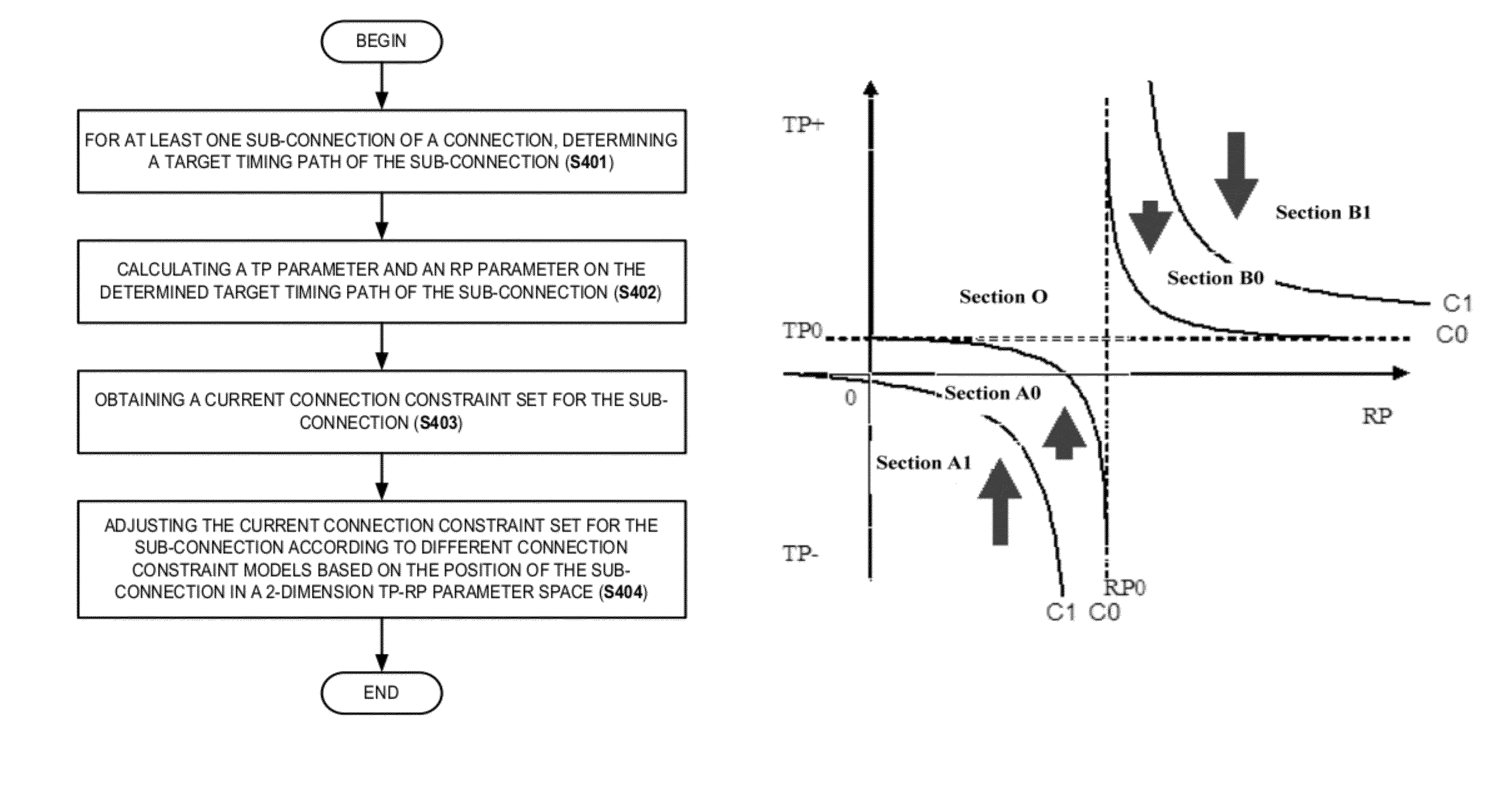
[0024]Embodiments will be described in more detail with reference to the accompanying drawings. Embodiments may, however, be embodied in various other forms and should not be construed as limited to the embodiments set forth herein. Rather, these embodiments are provided so that the disclosure is more thorough and complete, and will fully convey the scope of the disclosure to those skilled in the art.

[0025]Typically, an integrated circuit design can be deemed to be successful when both timing closure and physical closure are simultaneously achieved. During the design process, timing analyses can be carried out to ascertain whether the timing of the IC being designed is closed (e.g., whether timing closure is achieved). Typically, the timing analysis is relatively coarse at the start of the IC design cycle and becomes finer / closer to the timing of a real IC towards to the end design cycle. However, each at each step in the design process (e.g., as additional logic units are added to...


PUM


Abstract

Functionality can be implemented for optimizing connection constraints in an integrated circuit design. A target timing path associated with a first of a plurality of sub-connections of the integrated circuit is determined. A timing probability value and a route probability value associated with the first of the plurality of sub-connections is determined based, at least in part, on the target timing path associated with the first of the plurality of sub-connections. The timing probability value indicates a probability that timing closure is satisfied on the target timing path. The route probability value indicates a probability that a physical routing track on the target timing path associated with the first of the plurality of sub-connections resolves congestion. A current connection constraint associated with the first of the plurality of sub-connections is modified in accordance with a connection constraint model to which the first of the plurality of sub-connections corresponds.

Description

RELATED APPLICATIONS[0001]This application claims the priority benefit of Chinese Patent Application No. 201010532083.0 filed Oct. 29, 2010.BACKGROUND[0002]1. Technical Field[0003]Embodiments of the inventive subject matter generally relate to the design of an integrated circuit (IC) chip, and more specifically, to optimizing connection constraints in an integrated circuit design.[0004]2. Description of the Related Art[0005]Typically, large scale integrated circuits contain millions of logic gates. FIG. 1 shows the spatial structure of an existing IC chip, the bottom of the chip is a base layer consisting of transistors and the upper layer is a metal layer consisting of metal connections.[0006]In the design process of an integrated circuit, the first step is register transfer level (RTL) coding. The RTL coding is then encoded into a gate-level netlist containing devices and connections of chips by an IC design tool, such as a Synopsys® Design Compiler® tool. The process of encoding ...

Claims


Application Information

Patent Timeline
Patent Type & Authority Patents(United States)
IPC IPC(8): G06F17/50
CPCG06F17/5031G06F17/5077G06F2217/84G06F30/3312G06F30/394G06F2119/12
Inventor GE, LIANGLI, XIATANG, JIA LIANTANG, XIAO FENGXU, CHEN
Owner GLOBALFOUNDRIES US INC
Why Eureka
Try Eureka