Electrically conductive Kelvin contacts for microcircuit tester

a microcircuit tester and electrical conductor technology, applied in the direction of electronic circuit testing, measurement devices, instruments, etc., can solve the problems of reducing the value of the circuit board at that point, affecting the test results, so as to achieve the effect of limiting the possibility of flexur

Active Publication Date: 2013-10-15
JOHNSTECH INT
View PDF10 Cites 11 Cited by
  • Summary
  • Abstract
  • Description
  • Claims
  • Application Information

AI Technical Summary

Benefits of technology

[0004]The present invention is directed to equipment for testing microcircuits.
[0006]As microcircuits continually evolve to be smaller and more complex, the test equipment that tests the microcircuits also evolves. There is an ongoing effort to improve microcircuit test equipment, with improvements leading to an increase in reliability, an increase in throughput, and / or a decrease in expense.

Problems solved by technology

As microcircuits continually evolve to be smaller and more complex, the test equipment that tests the microcircuits also evolves.
Mounting a defective microcircuit on a circuit board is relatively costly.
Once mounted on a circuit board, removing a microcircuit is problematic because the very act of melting the solder for a second time ruins the circuit board.
Thus, if the microcircuit is defective, the circuit board itself is probably ruined as well, meaning that the entire value added to the circuit board at that point is lost.
Each microcircuit must be tested in a way that identifies all defective devices, but yet does not improperly identify good devices as defective.
Either kind of error, if frequent, adds substantial overall cost to the circuit board manufacturing process, and can add retest costs for devices improperly identified as defective devices.
Microcircuit test equipment itself is quite complex.
Because of the small size of microcircuit contacts and the spacings between them, even small errors in making the contact will result in incorrect connections.
Connections to the microcircuit that are misaligned or otherwise incorrect will cause the test equipment to identify the device under test (DUT) as defective, even though the reason for the failure is the defective electrical connection between the test equipment and the DUT rather than defects in the DUT itself.
A further problem in microcircuit test equipment arises in automated testing.
The sheer number of tests cause wear on the tester contacts making electrical connections to the microcircuit terminals during testing.
This wear dislodges conductive debris from both the tester contacts and the DUT terminals that contaminates the testing equipment and the DUTs themselves.
The debris eventually results in poor electrical connections during testing and false indications that the DUT is defective.
The debris adhering to the microcircuits may result in faulty assembly unless the debris is removed from the microcircuits.
Removing debris adds cost and introduces another source of defects in the microcircuits themselves.
If the test equipment is off line for extended periods of normal maintenance, the cost of testing an individual microcircuit increases.
Many times the alignment plate is separate from the housing that houses the contacts because it tends to wear and need replacing more often.
In general, it is impractical to solder and remove each electrical terminal on the microcircuit being contacted by a corresponding electrical probe on the testbed.
After testing, when the device under test is released, the terminals separate from the contacts and the circuits are broken.
First, in making the temporary contact with the ball terminals, the tester should not damage the S&P terminal surfaces that contact the circuit board, since such damage may affect the reliability of the solder joint for that terminal.
Tin-based solder alloys are likely to develop an oxide film on the outer surface that conducts poorly.
After testing, the chip is removed from the tester, and the mechanical and electrical contacts are broken.
For instance, it is not desirable to scrape the device I / O (leads, contacts, pads or balls), bend or deflect the I / O, or perform any operation that might permanently change or damage the I / O in any way.
There is currently a great deal of effort spent by tester manufacturers on the pad layouts.

Method used


Image

  • Electrically conductive Kelvin contacts for microcircuit tester
  • Electrically conductive Kelvin contacts for microcircuit tester
  • Electrically conductive Kelvin contacts for microcircuit tester

Examples


Embodiment Construction

[0086]A general summary of the disclosure follows.

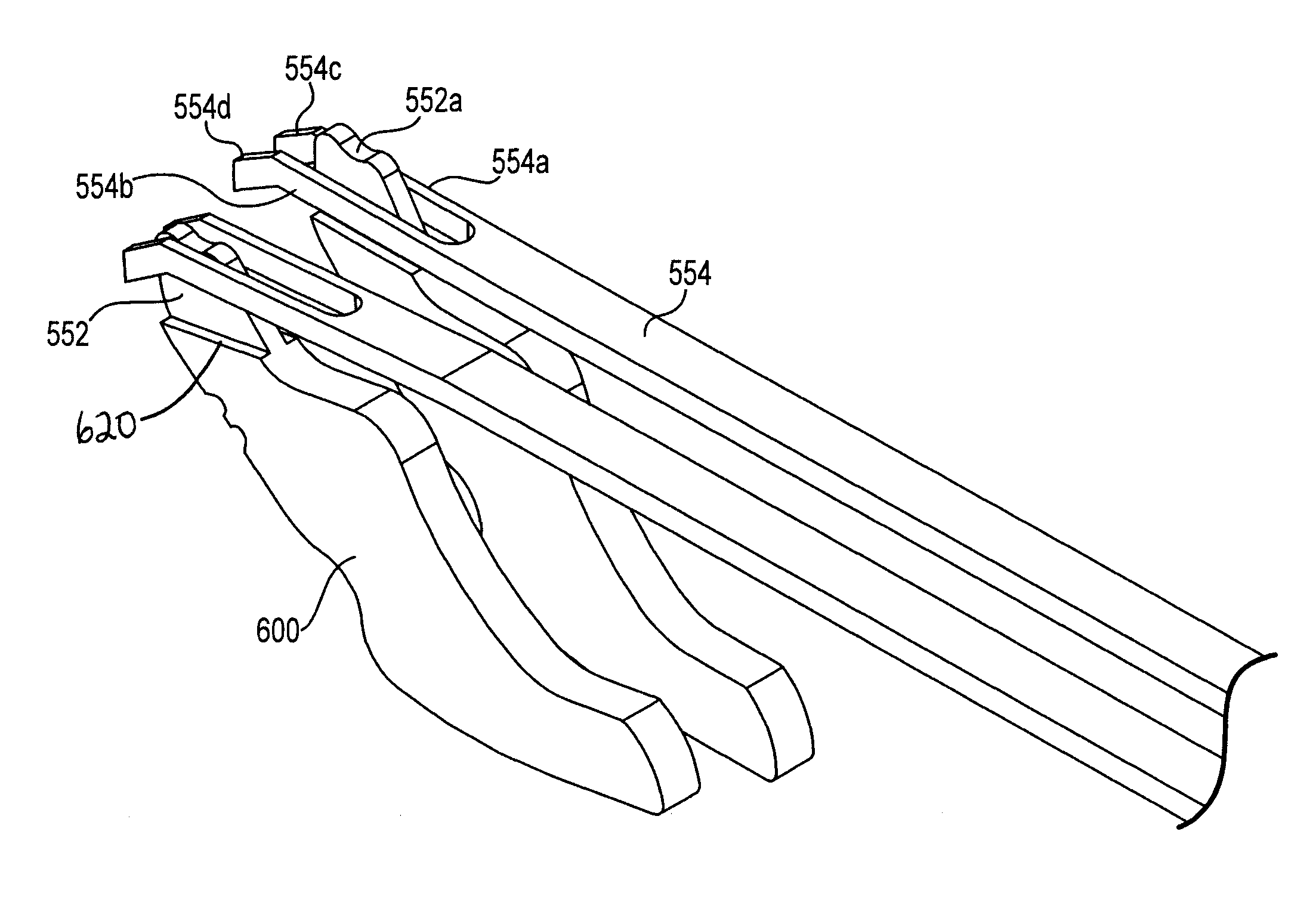
[0087]The terminals of a device under test are temporarily electrically connected to corresponding contact pads on a load board by a series of electrically conductive contacts. The terminals may be pads, balls, wires (leads) or other contact points. Each terminal that undergoes Kelvin testing connects with both a “force” contact and a “sense” contact, with each contact electrically connecting to a respective, single contact pad on the load board. The force contact delivers a known amount of current to or from the terminal, and the sense contact measures a voltage at the terminal and draws a negligible amount of current to or from the terminal. The sense contact partially or completely laterally surrounds the force contact, so that it need not have its own resiliency, though it may also be resilient in its own right. This helps keep the force contact in alignment by preventing lateral wobbling. In a first case, the sense contact has a...


PUM


Abstract

Terminals of a device under test are connected to corresponding contact pads or leads by a series of electrically conductive contacts. Each terminal testing connects with both a “force” contact and a “sense” contact. In one embodiment, the sense contact partially or completely laterally surrounds the force contact, so that it need not have its own resiliency. The sense contact has a forked end with prongs that extend to opposite sides of the force contact. Alternatively, the sense contact surrounds the force contact and slides laterally to match a lateral translation component of a lateral cross-section of the force contact during longitudinal compression of the force contact. Alternatively, the sense contact includes rods that have ends on opposite sides of the force contact, and extend parallel.

Description

CROSS-REFERENCE TO RELATED APPLICATIONS[0001]This application claims priority of provisional application No. 61 / 171,141, filed on 21 Apr. 2009, provisional application No. 61 / 257,236, filed on 2 Nov. 2009, and provisional application No. 61 / 307,501, filed on 24 Feb. 2010, which hereby is incorporated herein by reference in its entirety.STATEMENT REGARDING FEDERALLY SPONSORED RESEARCH OR DEVELOPMENT[0002]Not ApplicableBACKGROUND OF THE INVENTION[0003]1. Field of the Invention[0004]The present invention is directed to equipment for testing microcircuits.[0005]2. Description of the Related Art[0006]As microcircuits continually evolve to be smaller and more complex, the test equipment that tests the microcircuits also evolves. There is an ongoing effort to improve microcircuit test equipment, with improvements leading to an increase in reliability, an increase in throughput, and / or a decrease in expense.[0007]Mounting a defective microcircuit on a circuit board is relatively costly. Ins...

Claims


Application Information

Patent Timeline
Patent Type & Authority Patents(United States)
IPC IPC(8): G01R31/20G01R1/073
CPCG01R1/0466G01R1/07378G01R1/067G01R31/28
Inventor ERDMAN, JOEL N.SHERRY, JEFFREY C.MICHALKO, GARY W.
Owner JOHNSTECH INT
Why Eureka
Try Eureka