

Method for producing piezoelectric composite substrate and method for producing piezoelectric element
a composite substrate and piezoelectric technology, applied in the direction of after-treatment details, generators/motors, superimposed coating processes, etc., can solve the problem of risk of damaging the bonding surface, achieve little pyroelectricity, improve productivity, and prevent damage to the bonding surface
- Summary
- Abstract
- Description
- Claims
- Application Information
AI Technical Summary
Benefits of technology
Problems solved by technology
Method used
Image

Examples
first preferred embodiment
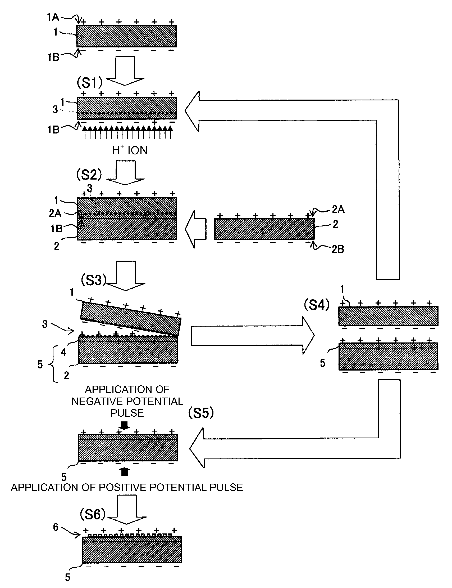
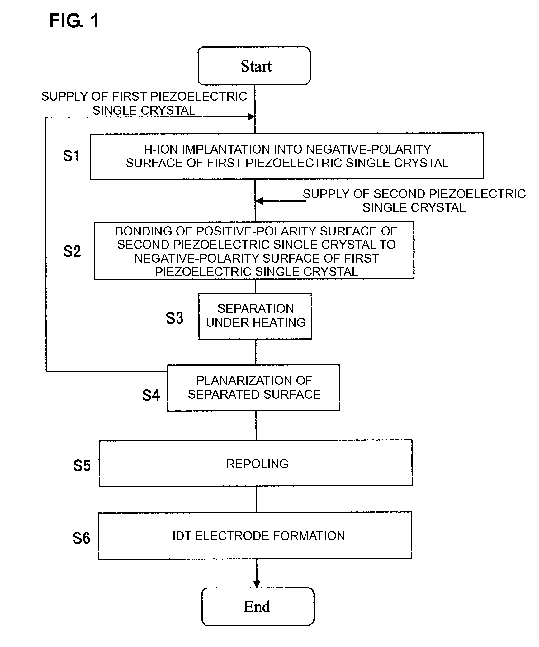
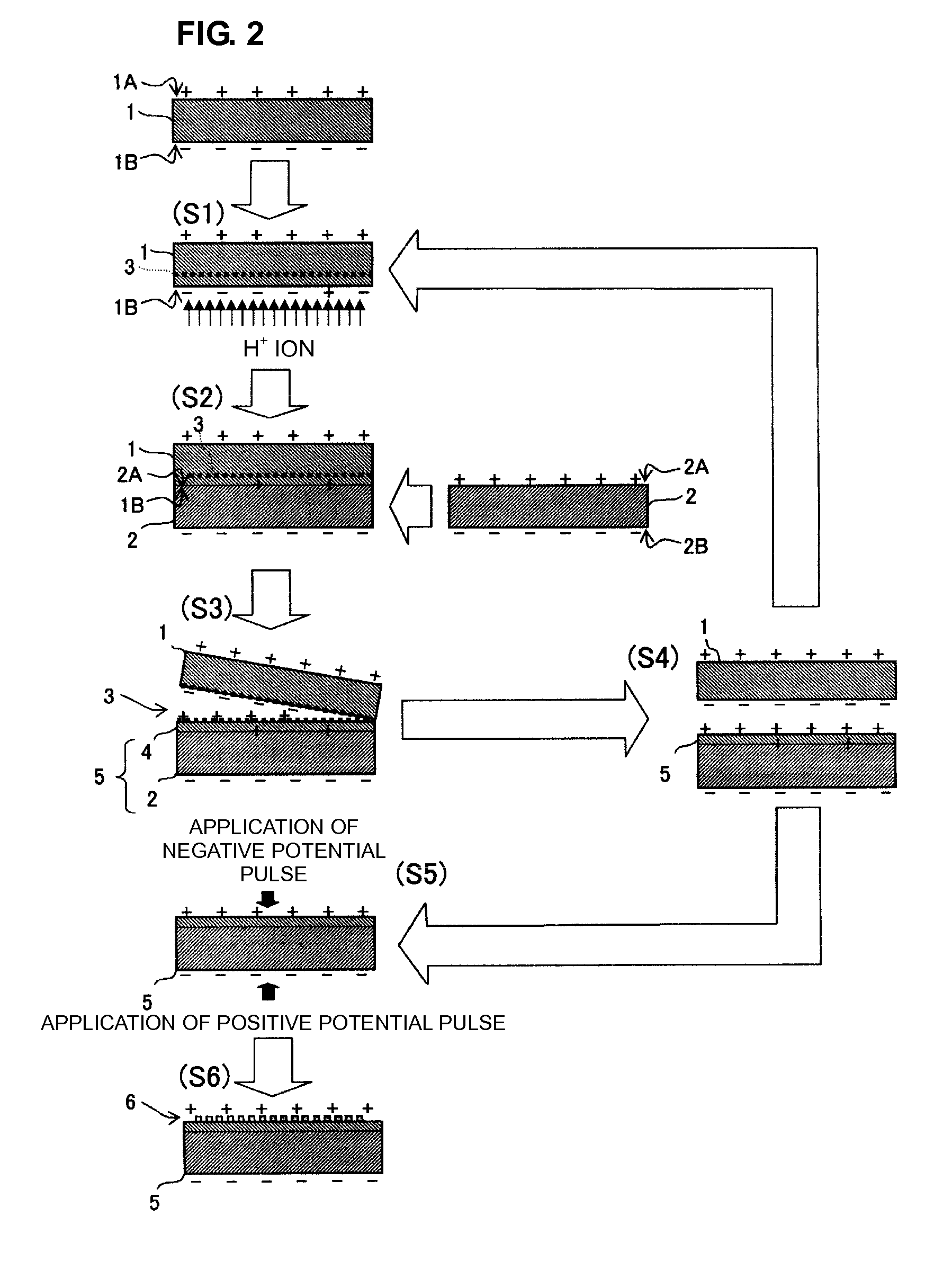
[0030]A method for producing a piezoelectric composite substrate according to a first preferred embodiment of the present invention will be described below with reference to a method for producing a surface acoustic wave resonator as an example.
[0031]FIG. 1 illustrates a flow chart of a method for producing a surface acoustic wave resonator according to this preferred embodiment of the present invention. FIG. 2 is a schematic view illustrating a piezoelectric composite substrate, a piezoelectric single crystal material, and a support substrate in steps in the flow chart according to this preferred embodiment of the present invention.
[0032]In this preferred embodiment, a 42° Y cut LiTaO3 substrate is preferably used as a first piezoelectric single crystal material 1, for example. Thus, the crystal axis of the first piezoelectric single crystal material 1 is inclined at 42° to the direction normal to a main surface, and the polar axis is inclined at 48° to the direction normal to the ...
second preferred embodiment
[0049]A method for producing a piezoelectric composite substrate according to a second preferred embodiment of the present invention will be described below with reference to a method for producing a surface acoustic wave resonator as an example.
[0050]FIG. 3 illustrates an example of the structure of a piezoelectric composite substrate 15 produced in this preferred embodiment.
[0051]The piezoelectric composite substrate 15 includes piezoelectric single crystal materials 11 and 12, a Si base 17, and an intermediate layer electrode pattern 16. Each of the piezoelectric single crystal materials 11 and 12 preferably has a thickness of about 0.1 μm to about 9.9 μm, for example. The Si base 17 preferably has a thickness of about 0.5 mm and is connected to the piezoelectric single crystal material 12. A vibration space 15A is exposed at a bonding surface between the Si base 17 and the piezoelectric single crystal material 12, the vibration space 15A being formed by removing a sacrificial la...
PUM
| Property | Measurement | Unit |
|---|---|---|
| temperature | aaaaa | aaaaa |
| thickness | aaaaa | aaaaa |
| roughness | aaaaa | aaaaa |
Abstract
Description
Claims
Application Information