THz antenna array, system and method for producing a THz antenna array

a technology thz antenna, applied in the field of thz antenna array, can solve the problems of affecting the performance of the antenna arrangement, comparatively inflexible methods, and high cost and error risk, and achieve the effect of increasing efficiency

Inactive Publication Date: 2013-11-12
RWTH AACHEN UNIV
View PDF12 Cites 6 Cited by
  • Summary
  • Abstract
  • Description
  • Claims
  • Application Information

AI Technical Summary

Benefits of technology

[0012]This is where the invention comes in, whose object is to specify a THz antenna array and a method for producing it which has improved properties and in particular is simplified with respect to known arrays and production methods.
[0019]Accordingly, the concept of the invention provides direct decoupling of the THz-active elements in the array, that is to say the THz antennae or THz antenna structures, according to which a lateral region between neighbouring THz antennae in the array are of practically non-photoconductive structure. In doing this the invention has recognised that optical generation of photoconductive charge carriers in the lateral region between neighbouring THz antennae in the array is intrinsically impossible or negligibly small so that in these regions inherently no emission of THz radiation can occur which could contribute to destructive distant field interference. By this means additional measures for antennae decoupling, such as location-dependent modulation of the optical excitation, whether done by binary grids, frequency mixing or optical blocking of the lateral regions between neighbouring THz antennae, are rendered unnecessary. In pursuit of this consideration the invention provides that a portion of the photoconductive region in the lateral region between neighbouring THz antennae in the array is removed, in particular completely removed. A corresponding THz antenna array exhibits in the latter case especially a photoconductive region which is restricted to a lateral extension which does not substantially go beyond the lateral extension of the spacing region or beyond the lateral extension of the spacing region and the electrodes. The THz antenna arrays provided according to the inventive idea and the corresponding production method inventively utilise the principle of the epitaxial lift-off method using comparatively thin photoconductive films. Accordingly, the structures emitting or detecting THz radiation forming elements of the array according to the concept of the invention can be adapted particularly flexibly and at low cost and without additional components to the most varied optical systems having full-surface optical excitation. It has been shown that the emission power or detection sensitivity is optimised in comparison with hitherto known THz antenna arrays. It has been shown that a THz antenna array according to the concept of the invention usually exhibits dark current reduced by at least 50% which additionally increases the consumption or sensitivity of a detector. Moreover, the disadvantages of the state of the art identified at the outset are largely avoided. If within the framework of special applications it should nevertheless be required to have additional location-dependent modulation of the optical excitation the proposed concept affords the advantage of an enlarged tolerance range for fine adjustment of a frequency-mixing optical excitation or a binary grid. Additional optically screening layers of material are not necessary as a rule. Production of the THz antenna array according to the concept of the invention can be carried out particularly effectively and at low cost.
[0021]It has been shown that on account of the epitaxial lift-off method preferably employed in the production process for lifting off a processed structure of a THz antenna array from the starting material a semiconductor material is no longer essential in principle for the support substrate. Within the framework of refinements support substrates can be employed which possess properties optimised for an appropriate application. In particular it has proved to be advantageous for a lateral region between neighbouring THz antennae in the array to be comparatively low in absorption and / or dispersion in the THz frequency range. Furthermore, a lateral region between neighbouring THz antennae in the array may also be constructed to be optically transparent and / or non-conducting. Electrical losses or dispersion effects can advantageously be largely avoided both in the THz frequency range and in the optical range. It has proved particularly advantageous in this context for the lateral region between neighbouring THz antenna arrays to be formed by a substrate, in particular by a sapphire or quartz glass substrate. Insofar as the substrate need not necessarily be optically transparent undoped silicon, for example, is also suitable since this has relatively low absorption and / or dispersion in the THz range.
[0030]Other advantageous refinements of the THz antenna arrays may be gathered from the other subsidiary claims and primarily serve to increase efficiency. This is achievable by different measures alone or in combination in the array design and / or antenna design, improving optical excitation and functionalisation of the layers and / or surfaces of the THz antenna array and / or the THz antennae. Preferably a spacing of the THz antennae is chosen to be comparatively large, in particular λ / 2. A microlens or microlens array may be provided for focusing and directing the optical excitation. A functionalised arrangement of nanoparticles of high dielectric constant may serve to amplify the field.
[0035]Other preferred production steps may be gathered from the subsidiary claims and advantageously serve to increase efficiency.

Problems solved by technology

A problem with this is the decoupling of the individual THz antennae as elements of the array in order to prevent destructive interference of the THz distant field—as a rule, e.g. in finger structures, neighbouring elements in the array, e.g. two fingers in each case with intervening photoconductive material, are biased with reciprocal polarity.
For this reason this method proves to be comparatively inflexible, costly and susceptible to error.
A disadvantage of this is that the production of such structures is comparatively costly since among other things two additional layers of material for optically blocking off suitable regions of the THz antenna array have to be deposited—this at least involves an electric insulation layer for insulating the electrodes of neighbouring THz antennae and deposited on top of this a layer impermeable to light which usually takes the form of a metal layer.
The additional optically screening layers identified there may generally adversely affect the performance of the antenna arrangement.
This results in higher energy consumption by the THz antenna array in the case of a THz emitter or in lower sensitivity in the case of a THz detector.
Moreover, the production of such an array has proved to be comparatively costly.

Method used


Image

  • THz antenna array, system and method for producing a THz antenna array
  • THz antenna array, system and method for producing a THz antenna array
  • THz antenna array, system and method for producing a THz antenna array

Examples


Embodiment Construction

)

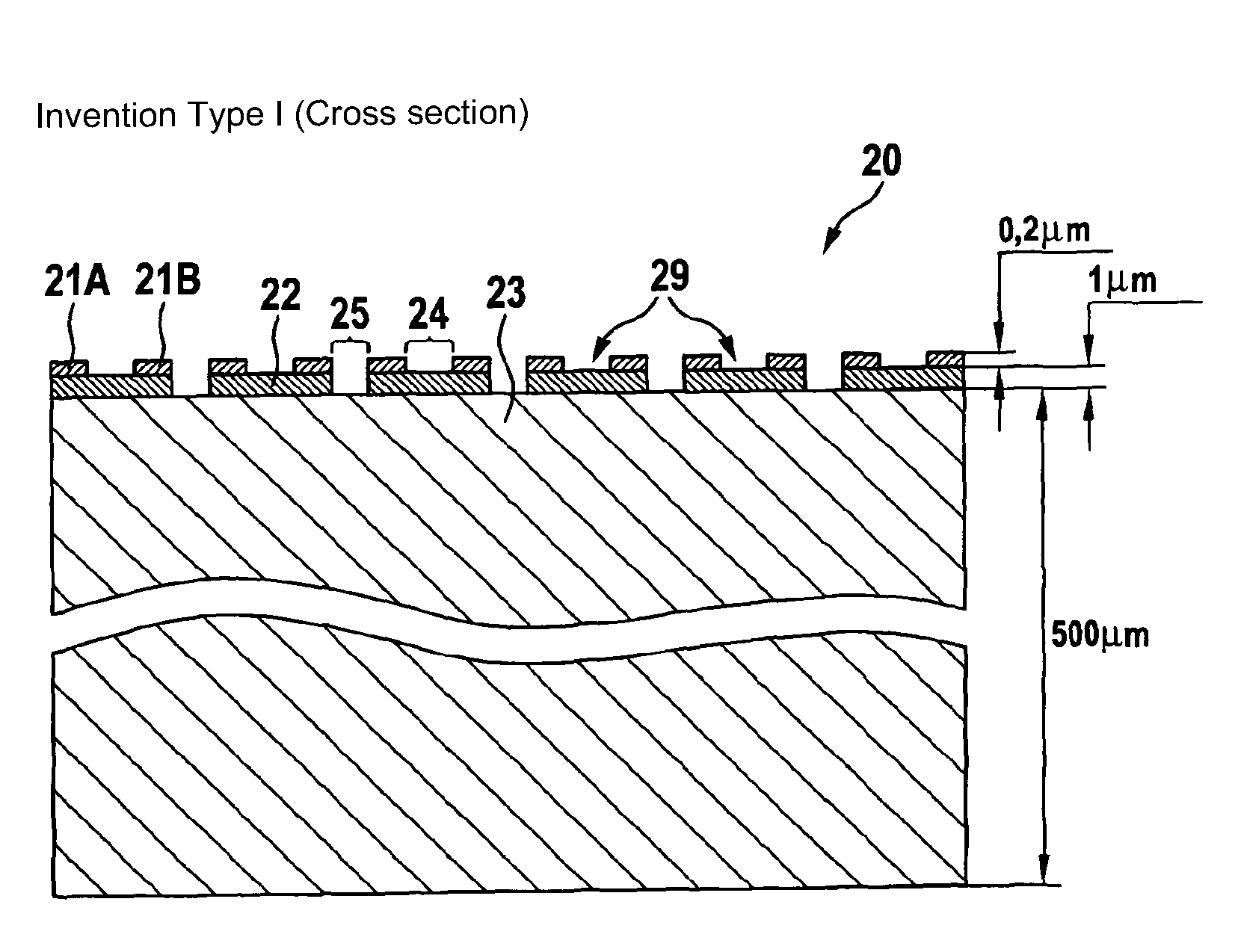
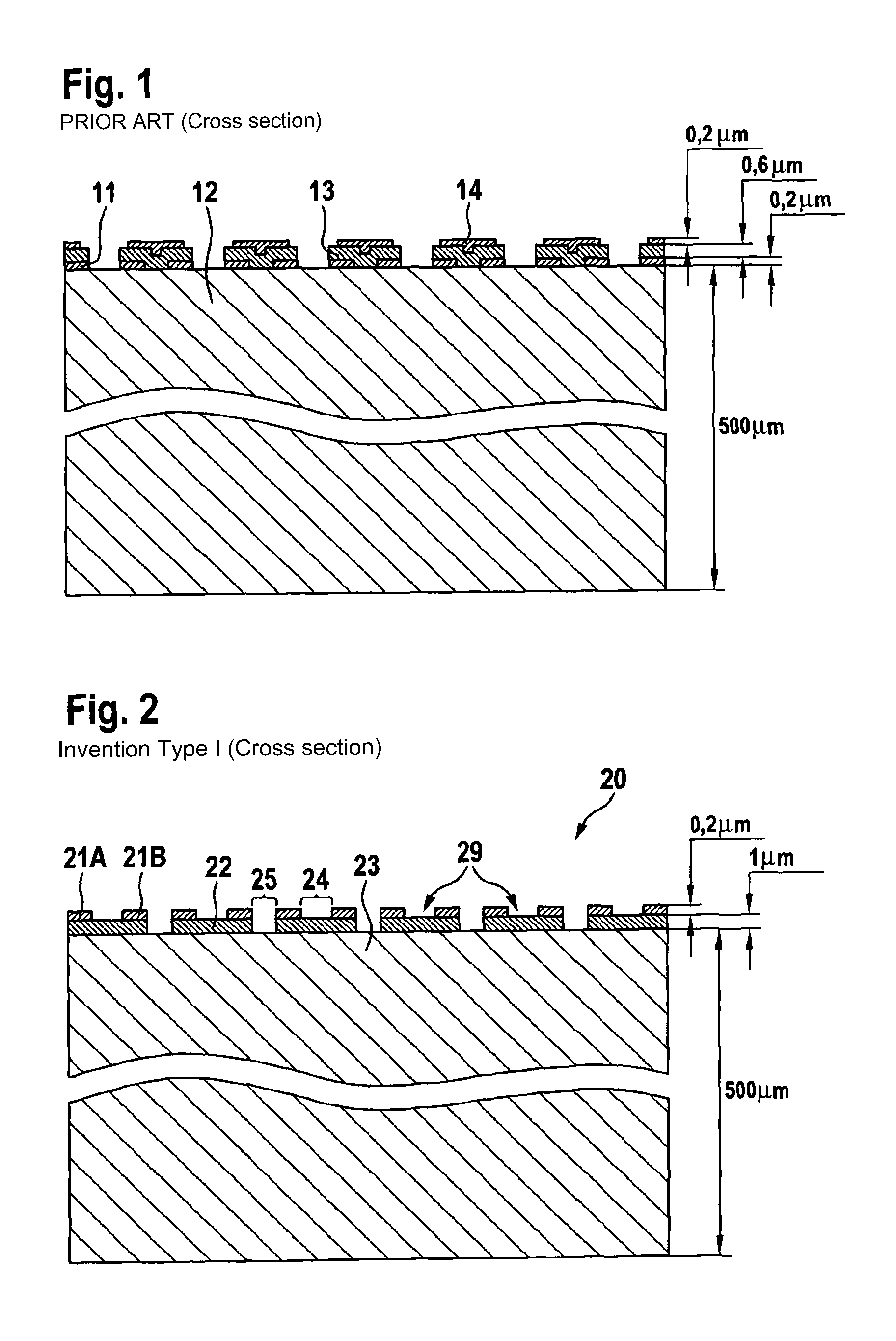
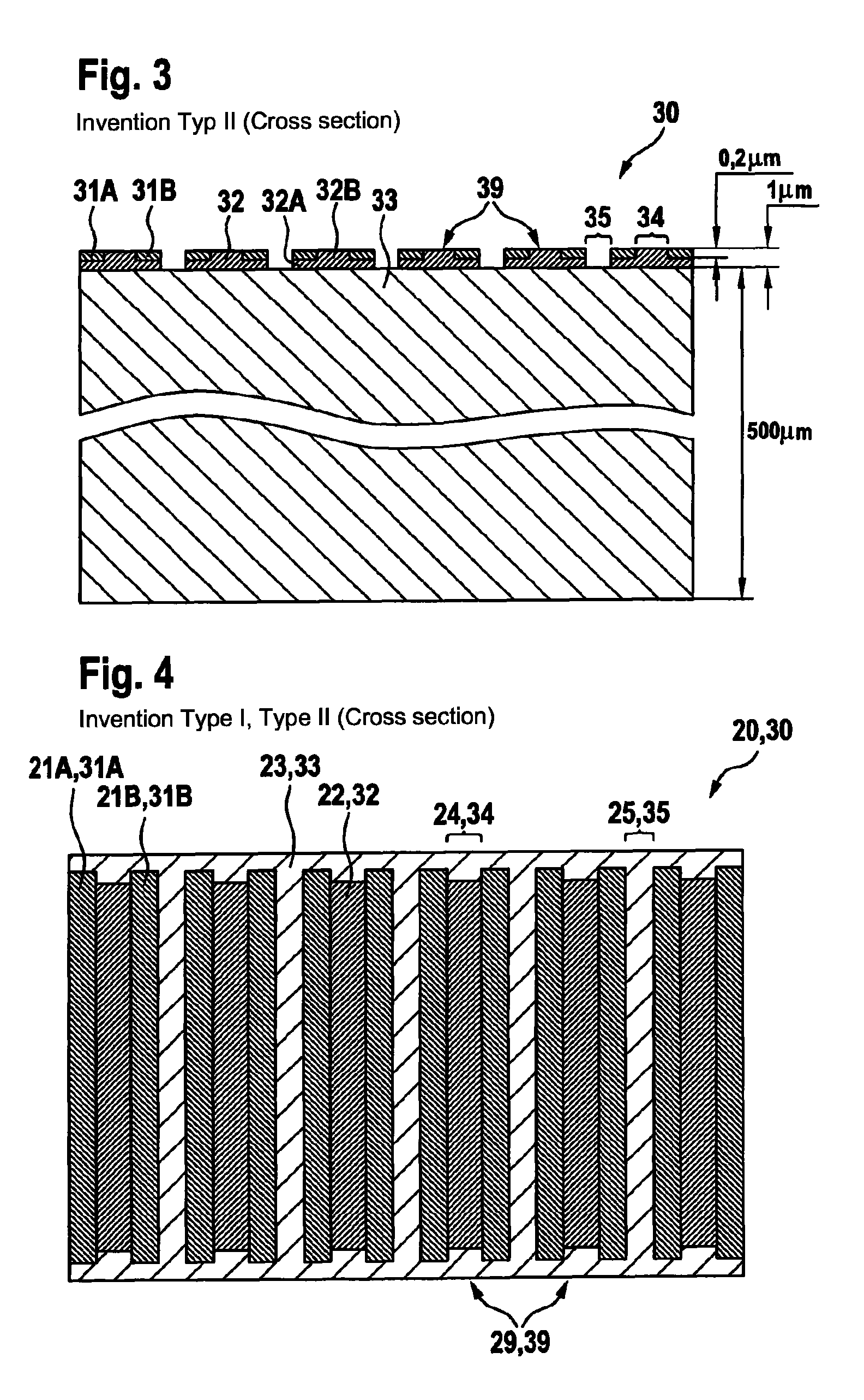
[0051]FIG. 1 shows a schematic cross-sectional illustration of a known THz emitter according to the article by Dreyhaupt et al. identified at the outset. Two intermeshing finger electrodes 11 are processed by optical lithography on the surface of a semiconductive GaAs wafer 12. The spacings of the fingers of the finger electrode 11 amount to 5 μm. The metallisation of a finger electrode 11 consists of 5 nm of chromium and 200 nm of gold. Another opaque metallised layer in the form of an optically [non-?]transparent metal layer 14 composed of chromium-gold covers each second finger electrode spacing. This second metal layer 14 is insulated from the first metal layer of the finger electrode 11 by an insulating layer 13 in the form of a polyimide layer approximately 2 μm thick or a silicon oxide layer 560 nm thick. The substrate in the form of the GaAs wafer 12 has a thickness of approximately 500 μm. When the finger electrodes are biased the electric field direction between successiv...


PUM

PropertyMeasurementUnit
wavelength rangeaaaaaaaaaa
wavelengthaaaaaaaaaa

Abstract

A THz antenna array has a plurality of THz antennae, a THz antenna having a photoconductive region and a first electrode and a second electrode which are arranged interspaced from each other via a spacer region that extends laterally across at least a part of the photoconductive region. In order to simplify the structure and facilitate its production, a lateral region between adjacent THz antennae of the array is not photoconductive. It is especially free from photoconductive material.

Description

RELATED APPLICATIONS[0001]This application is a 371 of PCT / EP2007 / 002790 filed Mar. 29, 2007, which claims priority under 35 U.S.C. 119 from GERMANY 10 2006 014 801.0 filed on Mar. 29, 2006, the contents of which are incorporated herein by references.BACKGROUND[0002](1) Field of the Invention[0003]The invention relates to a THz antenna array comprising a plurality of THz antennae, wherein a THz antenna has a photoconductive region and a first electrode and a second electrode which are arranged spaced apart from one another by a spacer region which extends laterally over at least a part of the photoconductive region. The invention further relates to a method for producing a THz antenna array comprising a plurality of THz antennae, wherein a THz antenna has a photoconductive region and a first electrode and a second electrode which are arranged spaced apart from one another by a spacer region which extends laterally over at least a part of the photoconductive region.[0004](2) Prior Ar...

Claims


Application Information

Patent Timeline
Patent Type & Authority Patents(United States)
IPC IPC(8): H01Q1/38H01Q13/10
CPCH01Q9/005Y10T29/49016
Inventor NAGEL, MICHAEL
Owner RWTH AACHEN UNIV
Why Eureka
Try Eureka