Scanning signal line drive circuit, shift register, and drive method of driving shift register

a drive circuit and signal line technology, applied in the direction of digital storage, instruments, computing, etc., can solve the problem of not being able to transfer video signals indicating pixels, etc., to reduce the size of the first switching element, reduce power consumption, and reduce the effect of siz

Active Publication Date: 2013-11-19
SHARP KK
View PDF34 Cites 7 Cited by
  • Summary
  • Abstract
  • Description
  • Claims
  • Application Information

AI Technical Summary

Benefits of technology

[0161]According to the first aspect of the present invention, in each bistable circuit that forms the shift register in the scanning signal line drive circuit of the display device, the first switching element has the configuration that the first electrode is connected to the first-node, the second electrode is supplied with the first clock signal and the third electrode is connected to the output-node. Hence, when the potential of the first-node rises based on the predetermined set signal and, then, the first clock signal changes from the Low level to the High level, the potential of the first-node further rises due to a parasitic capacitance between the first electrode and second electrode of the first switching element, so that the first switching element turns to the On state. As a result, the potential of the output-node rises, and the state signal indicating the first state is outputted from the output-node. The output-node discharging portion sets the state indicated by the state signal to the second state. On the other hand, when the first clock signal changes from the Low level to the High level in the case where the first-node is not charged, the potential of the first-node rises slightly due to the parasitic capacitance between the first electrode and second electrode of the first switching element. Each bistable circuit includes the first first-node discharging portion for discharging the first-node. The second-node connected to the first electrode of the second switching element included in the first first-node discharging portion is charged based on the third clock signal and discharged based on the fourth clock signal. Herein, the third clock signal is advanced in phase with respect to the first clock signal. Hence, when the first clock signal changes from the Low level to the High level in the non-selection period so that the potential of the first-node rises slightly, the second switching element included in the first first-node discharging portion is already in the On state. Accordingly, in the non-selection period, even when the potential of the first-node rises, the potential falls rapidly. Consequently, a leakage current in the switching element connected to the output-node becomes smaller than that in the conventional case. Thus, it is inhibited that an unnecessary electric current flows through the scanning signal line, which leads to reduction in power consumption.
[0162]Moreover, when the first clock signal changes from the High level to the Low level in the non-selection period, the potential of the first-node falls to a potential which is lower than a potential of a (negative) power supply voltage. Herein, since the timing at which the fourth clock signal changes from the Low level to the High level is earlier than the timing at which the first clock signal changes from the High level to the Low level, the second-node is in the discharged state and the second switching element is in the Off state at the point in time that the potential of the first-node falls to the potential which is lower than the potential of the power supply voltage. Hence, the potential of the first-node does not rise rapidly to the potential of the power supply voltage, but rises gradually to the potential of the power supply voltage. As a result, a negative bias voltage is applied satisfactorily to the first electrode of the first switching element in addition to a positive bias voltage through the period that the display device works. Consequently, the threshold shift in the first switching element becomes smaller than that in the conventional case. Accordingly, it is possible to reduce the size of the first switching element as compared with that in the conventional case, which allows size reduction in the display device.
[0163]Further, since the fourth clock signal is delayed in phase with respect to the first clock signal, in the selection period, the fourth clock signal changes from the Low level to the High level, so that the second-node is discharged. Herein, the second-node is connected to the first electrode of the second switching element having the second electrode connected to the first-node. As described above, since the period that the second switching element is set to the Off state in the selection period becomes longer than that in the conventional case, it is inhibited that the potential of the first-node falls in the selection period. If the potential of the first-node falls in the selection period, the fall of the scanning signal is delayed at the time of transition from the selection period to the non-selection period. According to the first aspect of the present invention, however, since the fall of the potential of the first-node in the selection period is inhibited, the scanning signal falls rapidly at the time of transition from the selection period to the non-selection period. Hence, it is inhibited that display defect occurs because the fall of the scanning signal becomes slow.
[0164]According to the second aspect of the present invention, the same effects as those of the first aspect of the present invention can be obtained with the configuration that each of the second-node discharging portion, the first second-node discharging portion and the first-node charging portion includes the switching element.
[0165]According to the third aspect of the present invention, since the second-node is discharged during the selection period, it is prevented that the potential of the first-node falls in the selection period. Moreover, by discharging the first-node after the termination of the selection period, it is inhibited that a leakage current is generated at the first switching element after the termination of the selection period.
[0166]According to the fourth aspect of the present invention, a scanning signal line drive circuit producing effects which are similar to those according to the third aspect of the present invention is realized through the configuration that the state signals outputted from the respective bistable circuits are used as the reset signal at the previous stage and the set signal at the subsequent stage.

Problems solved by technology

However, it is not possible to transfer video signals indicating pixel values for the plurality of lines at one time (the same time) through a single source bus line.

Method used


Image

  • Scanning signal line drive circuit, shift register, and drive method of driving shift register
  • Scanning signal line drive circuit, shift register, and drive method of driving shift register
  • Scanning signal line drive circuit, shift register, and drive method of driving shift register

Examples


Embodiment Construction

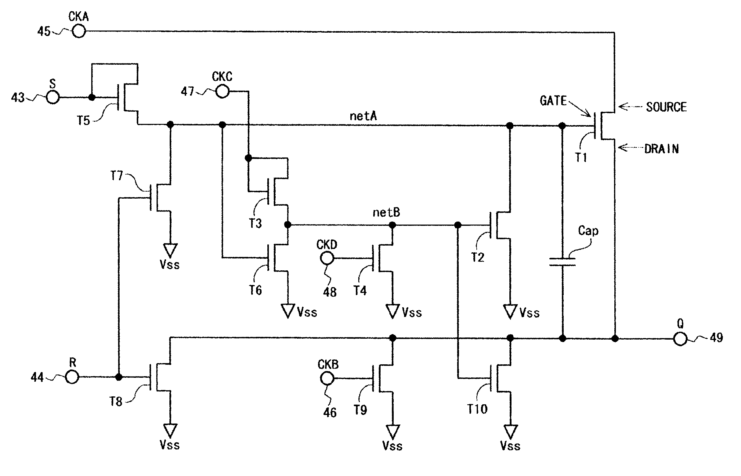
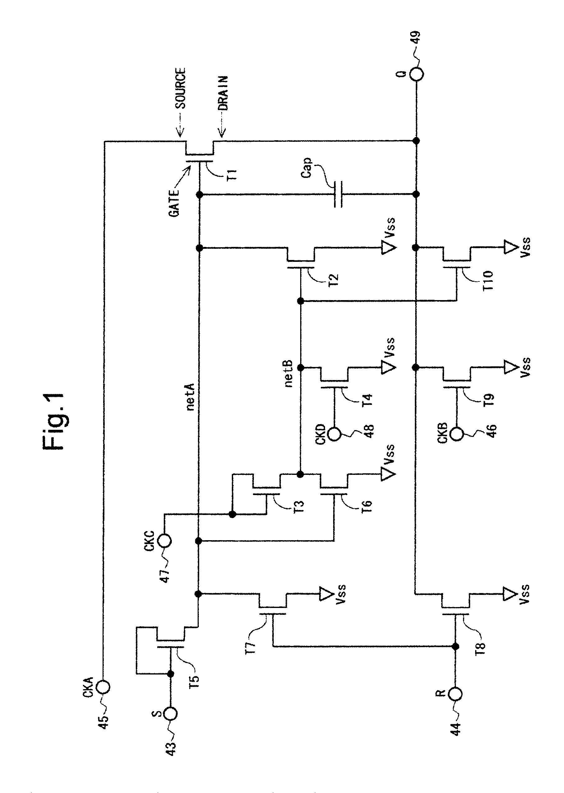
[0198]One embodiment of the present invention will be described below with reference to the attached drawings. In the following description, with regard to a thin-film transistor, a gate terminal (a gate electrode) corresponds to a first electrode, a source terminal (a source electrode) corresponds to a second electrode, and a drain terminal (a drain electrode) corresponds to a third electrode.

[0199]

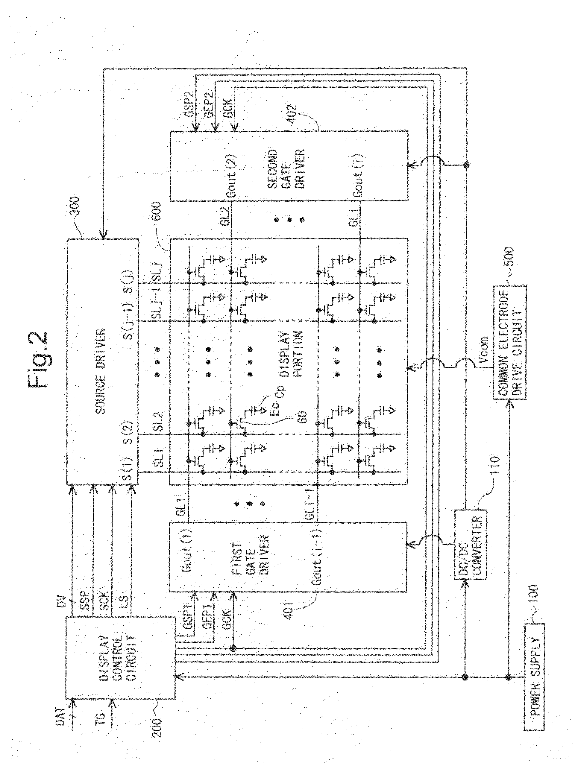
[0200]FIG. 2 is a block diagram showing a general configuration of an active matrix-type liquid crystal display device according to one embodiment of the present invention. As shown in FIG. 2, this liquid crystal display device includes a power supply 100, a DC / DC converter 110, a display control circuit 200, a source driver (a video signal line drive circuit) 300, a first gate driver (a first scanning signal line drive circuit) 401, a second gate driver (a second scanning signal line drive circuit) 402, a common electrode drive circuit 500 and a display portion 600. Typically, the displ...


PUM


Abstract

There is realized a scanning signal line drive circuit (in a display device) capable of, even in a case where a circuit in a shift register is formed using a thin-film transistor which is relatively large in off leakage, suppressing unnecessary power consumption due to a leakage current in the thin-film transistor. In at least one embodiment, bistable circuit that forms the shift register includes a thin-film transistor for raising a potential of an output terminal based on a first clock, a region netA connected to a gate terminal of the thin-film transistor, another thin-film transistor for lowering a potential of the region netA, and a region netB connected to a gate terminal of the other thin-film transistor. With this configuration, the potential of the region netB is raised based on a third clock which is advanced in phase by 90 degrees with respect to the first clock and is lowered based on a fourth clock which is delayed in phase by 90 degrees with respect to the first clock.

Description

TECHNICAL FIELD[0001]The present invention relates to a drive circuit and a drive method for an active matrix-type display device. More specifically, the invention relates to a shift register in a scanning signal line drive circuit that drives scanning signal lines arranged on a display portion in an active matrix-type display device, and a drive method therefor.BACKGROUND ART[0002]Liquid crystal display devices utilizing amorphous silicon (a-Si) thin film transistors (hereinafter referred to as “a-Si TFTs”) as driver elements have conventionally been known. In recent years, development of liquid crystal display devices utilizing microcrystalline silicon (μc-Si) thin film transistors (hereinafter referred to as “μc-Si TFTs”) as driver elements is moving forward. Mobility of microcrystalline silicon is greater than that of amorphous silicon, and the μc-Si TFTs can be formed by a process similar to that of the a-Si TFTs. For this reason, employment of the μc-Si TFTs as the driver elem...

Claims


Application Information

Patent Timeline
Patent Type & Authority Patents(United States)
IPC IPC(8): G09G3/36
CPCG09G3/3677G11C19/184G11C19/28G09G2310/0286G09G2330/021G09G2330/025
Inventor IWASE, YASUAKISAKAMOTO, MAYUKO
Owner SHARP KK
Why Eureka
Try Eureka