Replacement metal gate diffusion break formation

a technology of diffusion break and metal gate, applied in the field of semiconductors, can solve the problems of reducing image dimensions, affecting the quality of semiconductor devices, and not responding uniformly to feature types, and achieve the effect of eliminating device variability and high quality

Active Publication Date: 2013-12-17
GLOBALFOUNDRIES US INC
View PDF4 Cites 101 Cited by
  • Summary
  • Abstract
  • Description
  • Claims
  • Application Information

AI Technical Summary

Benefits of technology

[0007]In general, embodiments of the invention provide approaches for replacement metal gate (RMG) diffusion break formation. Specifically, a diffusion break is created after source/drain (S/D) formation, thereby allowing facet free and high quality S/D formation. A dummy gate body is removed selective to a capping layer and a GOx layer formed over a substrate, and the opening is then extended through the GOx l

Problems solved by technology

Unfortunately, all feature types do not respond uniformly.
This dichotomy has become especially troublesome, as image dimensions have shrunk.
However, at the 20 nm technology node and beyond, this approach suffers from one or more of the following deficiencies: a) poor source/drain growth at active region (Rx) a

Method used


Image

  • Replacement metal gate diffusion break formation
  • Replacement metal gate diffusion break formation
  • Replacement metal gate diffusion break formation

Examples


Embodiment Construction

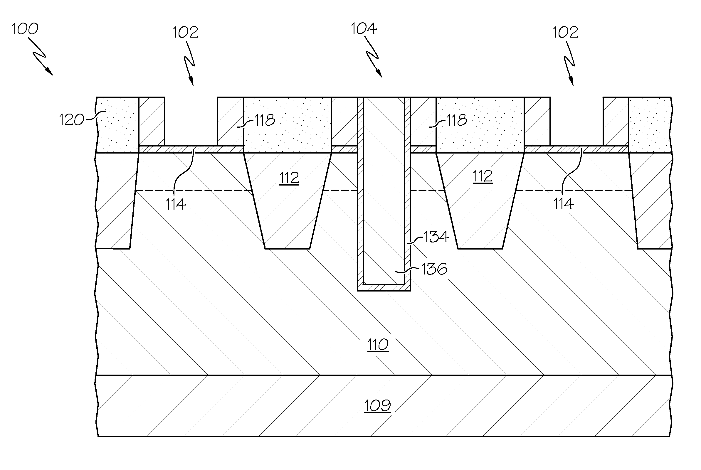
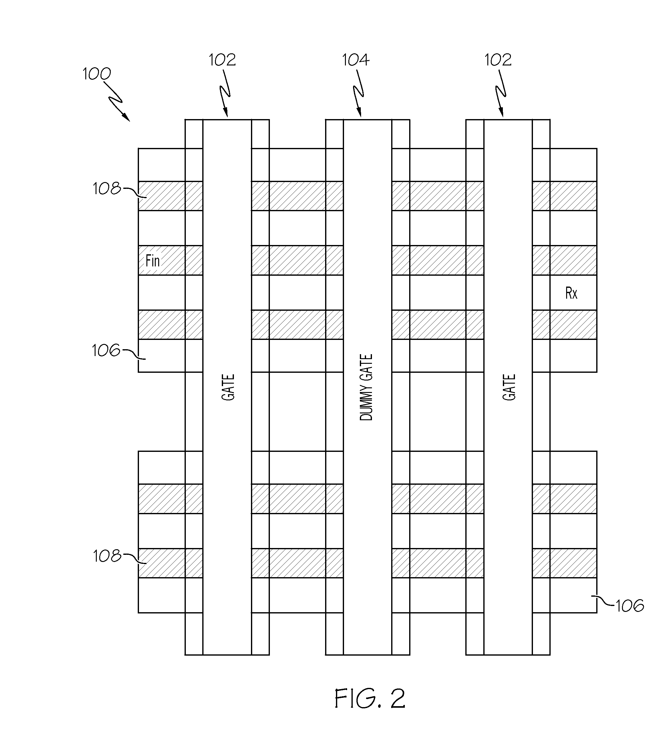
[0024]Exemplary embodiments will now be described more fully herein with reference to the accompanying drawings, in which exemplary embodiments are shown. Described are methods and techniques used in forming a diffusion break during replacement metal gate (RMG) formation. Specifically, exemplary embodiments provide approaches for creating the diffusion break after source / drain (S / D) formation, thereby allowing facet free and high quality S / D formation. A dummy gate body is removed selective to a capping layer and a GOx layer formed over a substrate, and an opening is then extended through the GOx layer and into the substrate by etching the dummy gate body selective to a sidewall section of the capping layer. Retaining the capping layer during the dummy gate body etch enables the diffusion break to be self-aligned to the gate and eliminates device variability due to S / D volume variations. Processing then continues with RMG poly open chemical mechanical planarization (POC) and poly op...


PUM


Abstract

Embodiments of the invention provide approaches for replacement metal gate (RMG) diffusion break formation. Specifically, a diffusion break is created after source/drain (S/D) formation, thereby allowing facet free and high quality S/D formation. A dummy gate body is removed selective to a sidewall section of a capping layer and a GOx layer formed over a substrate, and the opening is then extended through the GOx layer and into the substrate by etching the dummy gate body selective to the sidewall section of the capping layer. Retaining the capping layer during the dummy gate body etch enables the diffusion break to be self-aligned to the gate and eliminates device variability due to S/D volume variations. Processing then continues with RMG poly open chemical mechanical planarization (POC) and poly open planarization (POP).

Description

BACKGROUND[0001]1. Technical Field[0002]This invention relates generally to the field of semiconductors, and more particularly, to manufacturing approaches used in forming diffusion breaks during processing of integrated circuits and other devices.[0003]2. Related Art[0004]A typical integrated circuit (IC) chip includes a stack of several levels or sequentially formed layers of shapes. Each layer is stacked or overlaid on a prior layer and patterned to form the shapes that define devices (e.g., field effect transistors (FETs)) and connect the devices into circuits. In a typical state of the art complementary insulated gate FET process, such as what is normally referred to as CMOS, layers are formed on a wafer to form the devices on a surface of the wafer. Further, the surface may be the surface of a silicon layer on a silicon on insulator (SOI) wafer. A simple FET is formed by the intersection of two shapes, a gate layer rectangle on a silicon island formed from the silicon surface ...

Claims


Application Information

Patent Timeline
IPC IPC(8): H01L21/76
CPCH01L29/66545H01L21/76224H01L21/823431H01L21/845H01L29/66795H01L29/7848
Inventor BANNA, SRINVASAWEI, ANDY C.
Owner GLOBALFOUNDRIES US INC
Why Eureka
Try Eureka