Semiconductor memory device incorporating an interface chip for selectively refreshing memory cells in core chips

a memory cell and interface chip technology, applied in the field of memory controllers, can solve the problems of difficult selectively sending signals to specific core chips, difficult selectively performing refresh operations, etc., and achieve the effect of reducing the peak current in the refresh operation and increasing the efficiency of commands

Inactive Publication Date: 2013-12-31
LONGITUDE SEMICON S A R L
View PDF5 Cites 8 Cited by
  • Summary
  • Abstract
  • Description
  • Claims
  • Application Information

AI Technical Summary

Benefits of technology

[0012]According to the present invention, because each of the core chips performs a refresh operation by referring to the address information, a refresh operation can be selectively instructed to each of the core chips even when the refresh control signal is supplied in common to plural core chips. With this configuration, a peak current in the refresh operation can be reduced. Further, even when a certain core chip is performing a refresh operation, an arbitrary command (such as an active command) apart from a refresh command can be issued to other core chips that are not supposed to be refreshed. Therefore, the issuing efficiency of commands can be increased. Because a memory capacity to be refreshed by a refresh command for one time becomes small, a shortest issuing interval of a refresh command can be shortened even when it is necessary to comply with specifications such that a shortest issuing interval of a refresh command becomes long when a memory capacity is large.

Problems solved by technology

On the other hand, because data written in the memory cell is lost after a predetermined time, it is necessary to periodically perform a refresh operation.
Therefore, it becomes difficult to selectively send a signal to a specific core chip from an interface chip.
Consequently, in this type of semiconductor memory device, it is difficult to selectively perform a refresh operation by providing plural transmission paths of a refresh signal as described in Japanese Patent Application Laid-open No. 2000-30439.

Method used


Image

  • Semiconductor memory device incorporating an interface chip for selectively refreshing memory cells in core chips
  • Semiconductor memory device incorporating an interface chip for selectively refreshing memory cells in core chips
  • Semiconductor memory device incorporating an interface chip for selectively refreshing memory cells in core chips

Examples


Embodiment Construction

[0039]Preferred embodiments of the present invention will be explained below in detail with reference to the accompanying drawings.

[0040]FIG. 1 is a schematic cross-sectional view provided to explain the structure of a semiconductor memory device 10 according to the preferred embodiment of the present invention.

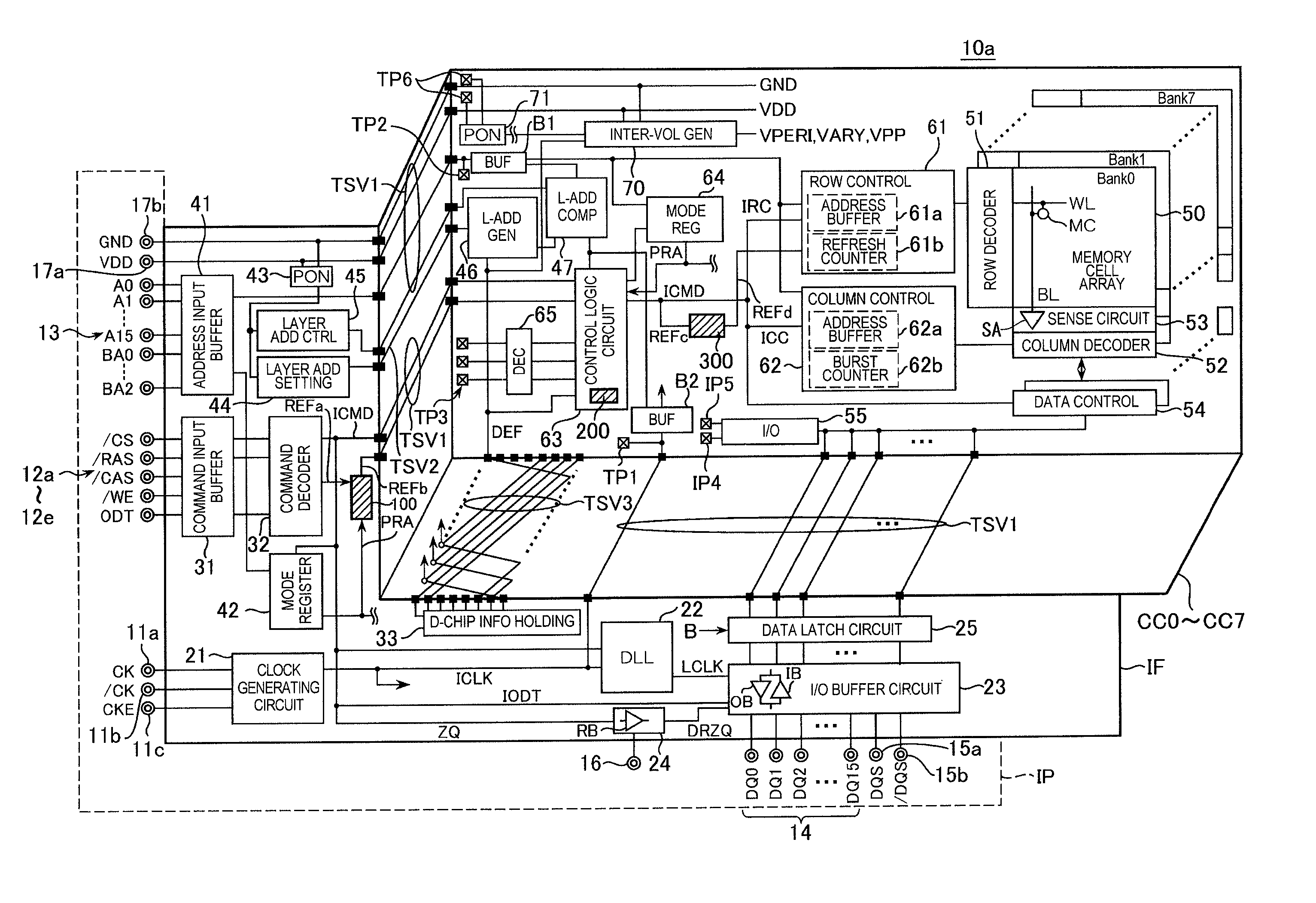
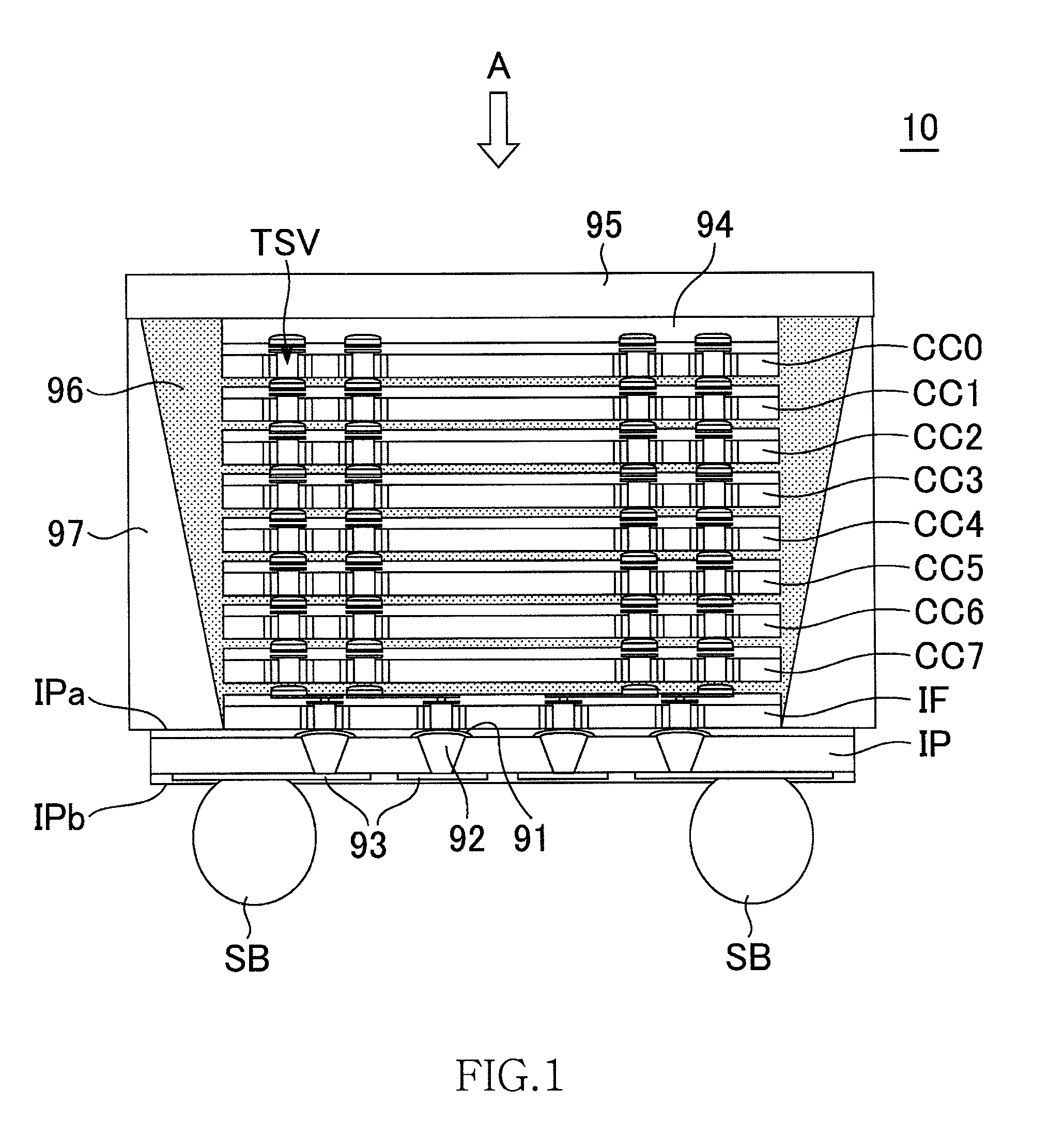
[0041]As shown in FIG. 1, the semiconductor memory device 10 according to this embodiment includes 8 core chips CC0 to CC7, an interface chip IF, and an interposer IP that are laminated. The 8 core chips CC0 to CC7 have a same function and structure and are manufactured using a same manufacture mask. The interface chip IF is manufactured using a manufacture mask different from that of the core chips. The core chips CC0 to CC7 and the interface chip IF are semiconductor chips including a silicon substrate and are electrically connected to adjacent chips in a vertical direction through plural Through Silicon Vias (TSV) penetrating the silicon substrate. The interposer IP is a c...


PUM


Abstract

In one embodiment, a semiconductor memory device receives a refresh command and address information, and supplies a refresh control signal and the address information in common to core chips. Each of the core chips includes a layer-address comparison circuit that determines whether the address information assigns an own core chip, and a refresh control circuit that refreshes an own memory cell based on the refresh control signal when the address information assigns the own core chip. With this arrangement, a memory capacity of a chip that is refreshed by a refresh command for one time is reduced, and therefore a shortest issuing interval of a refresh command can be shortened.

Description

BACKGROUND OF THE INVENTION[0001]1. Field of the Invention[0002]The present invention relates to a semiconductor memory device, a memory controller, and a data processing system including these, and more particularly relates to a semiconductor memory device that requires holding of data by a refresh operation, a memory controller that controls the semiconductor memory device, and a data processing system including the semiconductor memory device and the memory controller.[0003]2. Description of Related Art[0004]A DRAM (Dynamic Random Access Memory) as one of representative semiconductor memory devices has a memory cell constituted by one transistor and one capacitor. Therefore, an area occupied per one memory cell is small, and the DRAM has excellent characteristics such that a high integration can be obtained. On the other hand, because data written in the memory cell is lost after a predetermined time, it is necessary to periodically perform a refresh operation.[0005]In the refres...

Claims


Application Information

Patent Timeline
Patent Type & Authority Patents(United States)
IPC IPC(8): G11C7/00
CPCG11C29/50008G11C11/401G11C29/025G11C8/12G11C29/028G11C11/406G11C29/883G11C29/12G11C5/04G11C11/40615
Inventor HAYASHI, JUNICHIIDE, AKIRA
Owner LONGITUDE SEMICON S A R L
Why Eureka
Try Eureka